
ASML Deep Dive
A Near-Monopoly Lithography Franchise Powering Global Semiconductor Supply Chain with EUV Dominance and High-NA Optionality

Note: This report was originally completed on December 31st 2025, prior to its large price move. The analysis reflects information available as of that date and is intended to assess the company’s long-term business quality and economics rather than near-term earnings outcomes. The full PDF and accompanying financial model are available here.
Investment Thesis
ASML Holding N.V. is the global leader in photolithography and the central enabling chokepoint for advanced semiconductor manufacturing, combining a monopoly position in EUV with a dominant franchise in leading-edge DUV immersion. The company’s platform sits at the highest value density point of wafer-fab capex, where tool performance directly governs yield, cycle time, and the economics of node transitions. This strategic position is strengthened by multi-decade R&D, deep vertical integration across critical subsystems and software, and high switching costs embedded in customer process recipes. Financially, ASML has scaled to about €32 billion of LTM revenue as of December 2025, generated FY2024 net sales of ~€28.3 billion, and sustained structurally strong gross margins in the ~50.5% to 51.3% range through 2022–2024, improving to 52.7% in 9M 2025. Near-term results can be influenced by WFE capex phasing and geopolitics, particularly China exposure, but forward visibility is supported by a €33 billion backlog (Q3 2025), a book-to-bill near 1.0x (0.97x in Q3 2025), and a long-range revenue opportunity of ~€55 billion by 2030 alongside a 56% to 60% gross margin ambition.
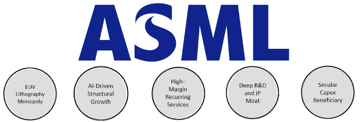
EUV Monopoly Drives Outsized Value Capture Per Tool: ASML is the only commercial supplier of EUV systems required for advanced logic and increasingly critical DRAM layers, concentrating the highest-value segment of lithography spending in a single vendor. EUV tools typically price at ~€150–200 million per system, creating exceptional revenue density relative to unit shipments. In Q3 2025, EUV contributed €2.1 billion, about 38% of net system sales (€5.6 billion) and ~28% of total net sales (€7.5 billion), from just 9 EUV tools out of 72 lithography systems shipped.
High-NA EUV Extends Scaling and Lifts Platform Economics: High-NA EUV increases numerical aperture (NA) from 0.33 to 0.55, enabling tighter pitches and supporting sub-2 nm patterning requirements that are not economically achievable with conventional optical approaches. System complexity and strategic importance translate into materially higher expected ASPs of ~€300–350 million per tool, expanding the revenue opportunity per node transition. Early deployments have begun, with broader ramps expected from 2026–2027 as leading customers align sub-2 nm process roadmaps.
DUV Immersion Remains a Critical Volume and Revenue Pillar: DUV immersion (TWINSCAN NXT) remains essential across advanced logic and memory for layers where EUV is unnecessary or less cost-effective, and for multi-patterning-intensive steps. Typical ASPs of ~€30–70 million provide meaningful system revenue and mix balance alongside EUV. In Q3 2025, DUV immersion accounted for ~52% of system sales, with 38 immersion tools shipped out of 72 lithography systems delivered.
Installed-base Services Increase Resilience and Recurring Cash Flows: Installed Base Management monetizes the growing global fleet through maintenance, spare parts, productivity upgrades, and field options, structurally reducing reliance on new tool cycles. In Q3 2025, services revenue was ~€1.96 billion, approximately one quarter of total quarterly net sales (€7.5 billion). By end-2025, the global EUV installed base exceeded 200 systems, expanding the long-duration service and upgrade annuity tied to high-availability fab operations.
Structural Margin Strength with a Credible Expansion Path: Gross margin expanded from mid-40s levels in 2015–2019 to 48.9% in 2020 and 52.7% in 2021, then held in the ~50.5% to 51.3% band during 2022–2024. In 9M 2025, gross margin rose to 52.7% and operating margin to 34.9%, supported by a richer mix and stronger upgrade activity. Long-term targets of 56% to 60% gross margin by 2030 are supported by EUV and High-NA scaling and deeper installed-base monetization.
Secular Demand Tailwinds from AI-led Node Intensity and Global Fab Expansion: AI accelerators and high-performance computing silicon are manufactured overwhelmingly at ≤5 nm nodes and drive higher lithography intensity per wafer through more critical layers and tighter overlay tolerances. AI-related semiconductor sales exceeded US$120 billion in 2024 and are expected to scale materially toward ~US$500 billion by 2028, sustaining leading-edge capacity additions and node migration. Policy-led fab buildouts in the US, Europe, and Japan support multi-year lithography demand, with new fabs typically exhibiting higher tool density and elevated service intensity during ramp.
Strong Cash Generation Supports Reinvestment Through the Cycle: Operating cash flow has consistently exceeded net income over the past decade, reflecting high earnings quality and disciplined working capital management. Capex has remained moderate at approximately 6% of revenue, allowing free cash flow to scale alongside earnings while sustaining heavy R&D investment. As of Q3 2025, cash of €5.1 billion versus debt of €2.7 billion implies ~€2.4 billion net cash, supporting capacity expansion, and long-cycle R&D. This strong cash profile also enables ASML to invest continuously in next-generation lithography while maintaining balance-sheet resilience and shareholder returns.
R&D Scale, IP Depth, and Balance-sheet Strength Reinforce Durability: R&D spending of approximately €4.3 billion in FY2024, representing about 14%–15% of revenue, and a similar intensity in Q3 2025 (€1.1 billion R&D spend on €7.5 billion of revenue) sustains a widening technology gap versus legacy competitors and supports continued roadmap execution. A patent estate of ~38,000 patents (as of 2025) and vertically integrated capabilities across sources, software, and inspection fortify barriers to entry and ecosystem lock-in.
Backlog and Bookings Support Strong Forward Visibility: Net bookings of €5.3 billion in Q3 2025 versus systems revenue of ~€5.5 billion imply a 0.97x book-to-bill, indicating order intake broadly aligned with shipments. Backlog of ~€33 billion as of Q3 2025 equates to roughly six quarters of revenue coverage at the Q3 run-rate. Delivery timing can still be rephased by customers due to long lead times and capex budgeting, but the backlog provides a substantial visibility buffer.
High Switching Costs and Process Lock-in Limit Competitive Risk: Lithography systems are deeply embedded in customer process flows, yield models, and qualification frameworks, making tool substitution operationally and economically prohibitive. Requalification cycles typically span 12–24 months and carry material yield and schedule risk at advanced nodes, deepening customer reluctance to switch vendors. With thousands of DUV systems and more than 200 EUV systems installed globally, ASML’s installed base further entrenches long-term customer dependence and service pull-through.
Technology Leadership Enabled by Vertical Integration: The internalization of critical subsystems through acquisitions such as Cymer (EUV light sources), Brion (computational lithography), and HMI (e-beam inspection) enables end-to-end co-optimization across exposure, modeling, and defect detection. This integration accelerates learning curves, shortens development cycles, and reduces dependency on external suppliers for performance-critical components. Vertical integration materially raises barriers to entry by requiring any potential competitor to replicate multiple complex technologies in parallel.
Valuation: ASML’s growth profile is supported by its near-monopoly position in lithography, which structurally links its revenue trajectory to global wafer-fab equipment (WFE) spending and an accelerating mix shift toward higher-value EUV, High-NA, and productivity-enhancing platforms. We apply a top-down revenue framework that allocates approximately 30% of global WFE spending to lithography, and then translate this spend into ASML revenue by applying EUV and DUV market-share assumptions, separating system sales from installed-base services, and anchoring unit volumes and average selling prices (ASP) within a coherent revenue bridge. Under this approach, we estimate total lithography spending of €28.55 billion in 2025, translating into €23.14 billion of combined EUV and DUV system sales and approximately €32.2 billion of total revenue, inclusive of installed-base services, upgrades, software, and other non-system contributions. Given ongoing tariff and policy uncertainty, alongside management’s indication that China’s revenue contribution is expected to normalize from the elevated levels seen in 2024–2025, we adopt more conservative near-term growth assumptions, resulting in an estimated €33.4 billion of revenue in 2026. Beyond this period, growth is increasingly driven by structural factors, including AI-led leading-edge logic investment, rising lithography intensity at advanced nodes, and a progressively richer mix of EUV productivity upgrades and High-NA deployments. These drivers support a revenue trajectory of approximately €55 billion by 2030, consistent with management’s stated €44–€60 billion long-term opportunity range. On profitability, we model 2025 gross and operating margins of 52.6% and 33.8%, respectively, followed by a normalization of approximately 140 basis points in 2026 as the contribution from high-margin immersion shipments to China moderates. Thereafter, we assume margin expansion resumes, driven by EUV and High-NA mix, operating leverage, and deeper installed-base monetization, reaching approximately 56% gross margin and 40% operating margin by 2030. Our valuation assumes a reinvestment-oriented capital allocation approach, with no explicit modeling of dividends or share repurchases, and normalized capital expenditure at 5% of revenue. Under a discounted cash flow (DCF) framework applying an 8.05% discount rate and a 1.5% terminal growth rate, these assumptions yield an intrinsic equity value of approximately $1,239 per share, implying meaningful upside relative to the current share price of $1,070.
Levers & Catalysts:
AI accelerator driven leading-edge fab expansion
High-NA EUV commercial ramp
EUV productivity and throughput upgrades
Installed-base service and upgrade monetization
Policy-backed US, EU, Japan fab buildouts
EUV penetration into advanced DRAM layers
Mix shift toward higher-ASP lithography systems
Company Overview
ASML Holding N.V. is a Dutch multinational corporation and a global leader in semiconductor equipment supply chain, specializing in the design and manufacture of photolithography systems used to produce integrated circuits. Founded in 1984, ASML has grown from a small venture into an indispensable player in the semiconductor supply chain. It is the world’s largest supplier of lithography machines and notably the sole provider of cutting-edge extreme ultraviolet (EUV) lithography tools needed for the most advanced chip manufacturing. This unique position gives ASML a near-monopolistic edge in its field.
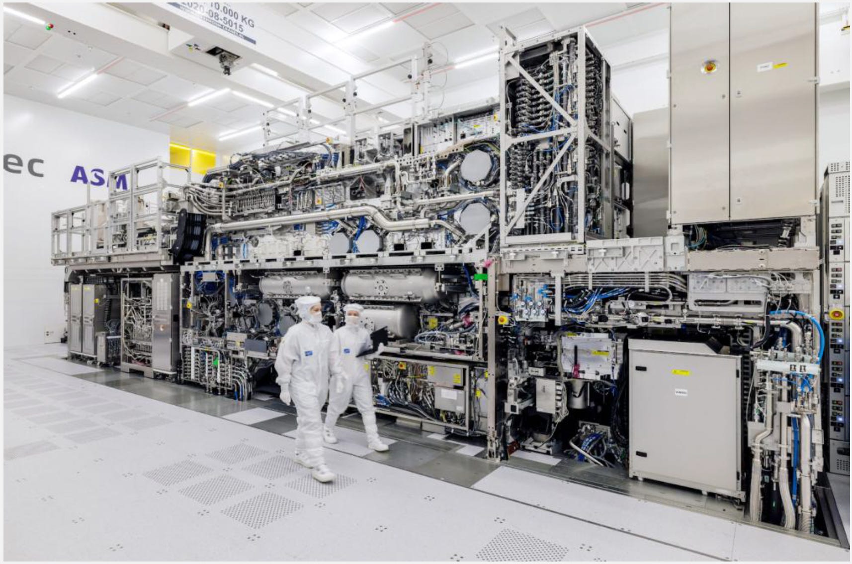
Exhibit 1: ASML’s High-NA EUV Lithography Machine. Source: ASML Holding
ASML operates in the highly specialized market of semiconductor fabrication equipment. Its core business is the design, manufacturing, and servicing of photolithography systems – the machines that project circuit patterns onto silicon wafers in chip production. These systems, often called “scanners,” are extraordinarily complex and expensive, typically selling for tens of millions of euros each (with the latest models costing up to hundreds of millions). ASML’s revenue comes primarily from new equipment sales, but it also generates substantial recurring income by providing maintenance, upgrades, and support services to customers via a global service network. Additionally, ASML offers refurbished used systems (for customers who want lower-cost legacy equipment) and sells software and metrology tools that complement its lithography products. As of the last twelve months (LTM), December 2025, the company’s annual revenue was about €32 billion, and its market capitalization (around $433 billion) made it one of Europe’s most valuable technology companies.
ASML’s Historical Evolution
ASML Holding was founded on April 1, 1984, as a joint venture between Dutch electronics company Philips and chip equipment firm ASM International. The new company, originally named ASM Lithography, began humbly in a leased shed in Eindhoven and launched its first product, the PAS 2000 wafer stepper, that same year. Early growth was supported by its parents’ (Philips) funding. By 1985, ASML had built its first factory in Veldhoven and, in 1986, introduced the PAS 2500 stepper, featuring an alignment technology co-developed with lens partner Carl Zeiss that laid the groundwork for future innovations. Despite technical progress, ASML struggled financially in the late 1980s amid a downturn in the electronics industry. ASM International withdrew its stake, and Philips undertook major cost-cutting, bringing ASML close to collapse. A last-minute infusion from Philips’ board in 1988 kept the venture alive. That same year, the company spun out as an independent entity, officially renamed ASML.
ASML’s fortunes turned in the early 1990s with a breakthrough product. In 1991, it launched the PAS 5500 lithography system, a high-throughput step-and-scan tool that proved extremely successful. Micron Technology, a major memory chip maker, became an early adopter of the PAS 5500, and its performance helped establish ASML as a serious competitor to then-dominant Japanese rivals Nikon and Canon. Building on this success, ASML went public in 1995 and fully separated from Philips, listing its shares on the Amsterdam and NASDAQ exchanges.
The early 2000s saw ASML expand via acquisitions and new technology. In 2000, ASML acquired Silicon Valley Group (SVG), a U.S. lithography equipment maker, to broaden its portfolio of 193 nm deep-ultraviolet tools and gain access to SVG’s EUV research. Around the same time, ASML introduced its TWINSCAN platform, a dual-stage wafer scanner design that enabled continuous lithography and higher throughput. It also pioneered immersion lithography (submerging the wafer in fluid to enhance optical resolution), which TSMC first used in volume production at the 90 nm node in 2004. These innovations helped ASML overtake competitors: by 2002, it had become the world’s largest supplier of photolithography systems. The mid-2000s solidified ASML’s lead, though the 2008 financial crisis caused a temporary sales slump and layoffs. The company rebounded strongly by 2010 as demand for advanced chip equipment returned.
During the 2010s, ASML made bold strategic moves to secure its technological edge. In 2012, recognizing the daunting costs of EUV development, major customers Intel, TSMC, and Samsung invested in ASML as part of a co-investment program. Intel alone paid $4.1 billion for a ~15% stake to accelerate 450 mm wafers and EUV, and ASML invited others to take a 10% share, emphasizing the industry’s reliance on ASML’s roadmap. That same year, ASML acquired Cymer, its long-time U.S. laser light source supplier, to bring critical EUV light source technology in-house. In 2016, ASML expanded into pattern verification and metrology by acquiring Taiwan’s Hermes Microvision (HMI) for $3.1 billion, adding e-beam inspection tools to its portfolio. ASML also continued refining EUV, shipping its first pilot EUV scanners in the early 2010s and working with chipmakers on incremental improvements. By the late 2010s, EUV became viable for high-volume manufacturing: in 2018, TSMC and Samsung adopted ASML’s EUV scanners for production at the 7 nm node, a pivotal milestone after decades of development.
In recent years, ASML’s dominance has only grown. In 2020, it acquired Berliner Glas Group, a German optical components manufacturer, to secure the supply of high-precision glass and mirrors needed for EUV systems. By 2021, ASML was recognized as having a near-monopoly in advanced lithography equipment – the only supplier of EUV tools and the primary source of leading-edge DUV scanners used by top chipmakers. In 2023, ASML shipped the first next-generation EUV system featuring a 0.55 numerical aperture (NA) optics system (versus 0.33 NA in current EUV scanners). This new platform, called the EXE series, is known as “High-NA EUV” and includes novel optics and faster wafer stages. High-NA EUV is expected to enable even smaller transistor geometries for future chip nodes (beyond ~2 nm), extending ASML’s technology leadership. While ASML’s technical trajectory remains strong, global trade dynamics have introduced geopolitical complexities. Despite such challenges, ASML stands as a highly innovative company at the forefront of semiconductor manufacturing technology, far evolved from its humble beginnings in a Dutch shed.
ASML today operates in dozens of locations worldwide, having over 60 service and support sites across 16 countries, reflecting the global nature of the semiconductor industry. Major regional offices and training centers are located in semiconductor hubs such as Taiwan, South Korea, China, Japan, and the United States, among others. For example, ASML’s presence in Taiwan supports TSMC’s fabs; in South Korea, it supports Samsung and SK Hynix; and in the US, it serves Intel and other clients. This extensive global footprint enables ASML to provide timely maintenance and support, which is critical because any downtime of a lithography tool can be extremely costly for chipmakers. Manufacturing and assembly are also globally distributed: while final system integration and testing occur in Veldhoven, Netherlands, the company also produces or sources subassemblies in other locations (such as Wilton, Connecticut for certain module manufacturing, and Linkou, Taiwan for some refurbishments), and it operates development centers in places like Silicon Valley and San Diego. The company’s worldwide workforce of over 40,000 employees is highly globalised, comprising more than 140 nationalities, which helps ASML tap into a broad engineering talent pool.
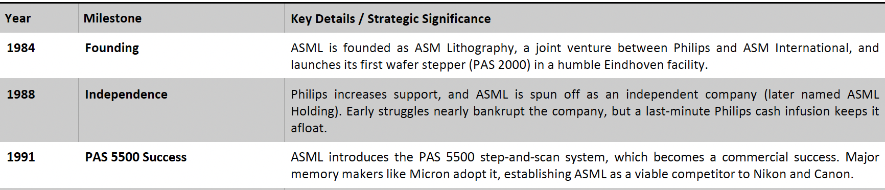
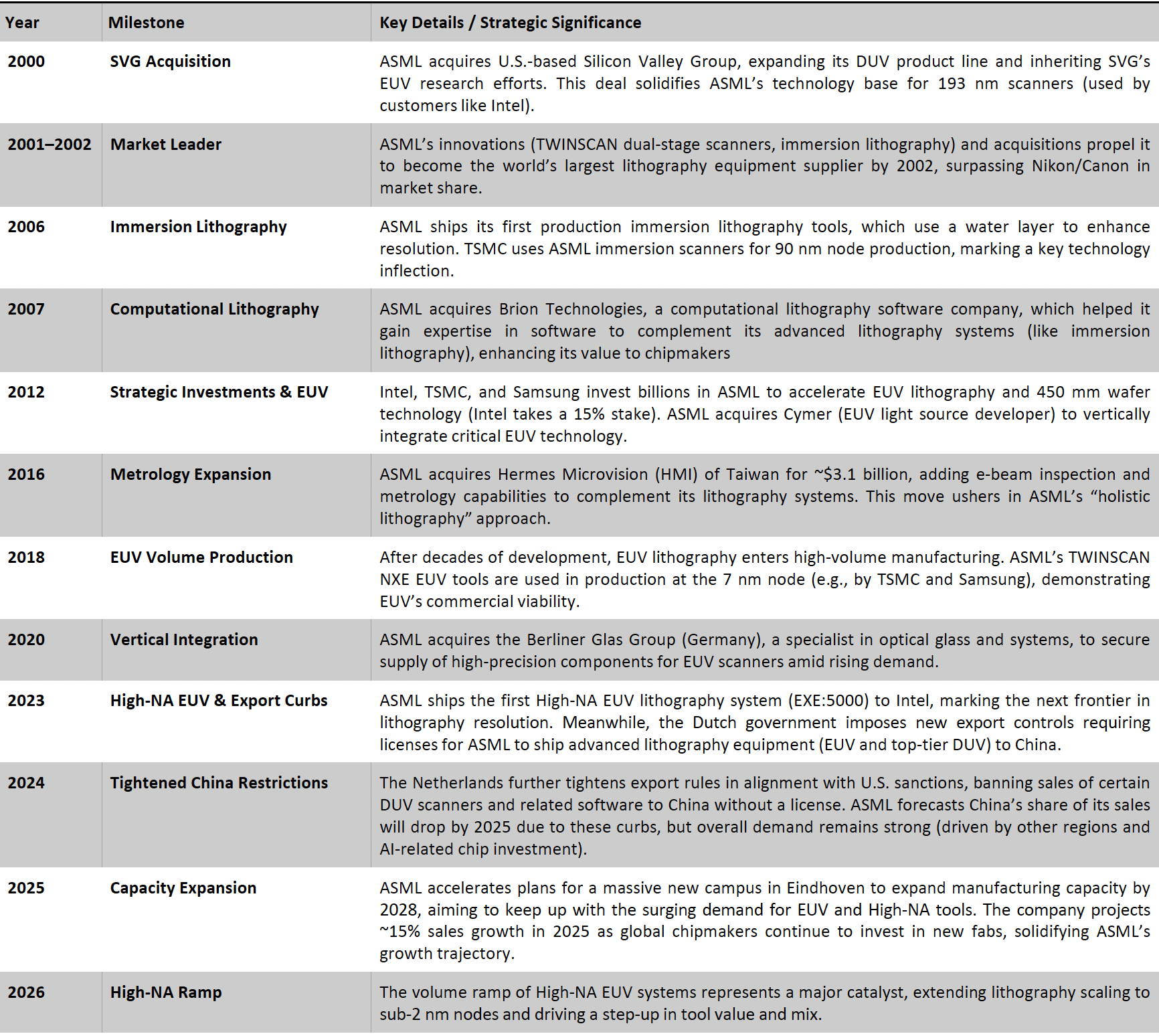
Exhibit 2: ASML’s Key Strategic Milestones. Source: Business Deep Dives Research
An Irreducible Layer: Why Lithography Defines Semiconductor Progress
Lithography is the foundational patterning process in semiconductor manufacturing, responsible for transferring circuit designs onto silicon wafers with exceptional spatial precision. It operates by projecting a highly controlled light source through a patterned photomask onto a thin, photosensitive chemical layer known as a photoresist. This exposure process defines the critical dimensions and geometries of transistors and interconnects, making lithography the single most influential step in determining device performance, wafer yields, power efficiency, and the cost per transistor.
Exhibit 3: Photolithography Machine (Left), Photolithography Technique in Action (Right). Source: BranchEducation
Lithography is the foundational patterning step in semiconductor manufacturing, enabling the precise transfer of circuit designs onto silicon wafers with nanometer-scale accuracy
As semiconductor technology nodes have progressively shrunk into the nanometer regime, lithography has become the dominant enabler of device scaling and the primary mechanism through which the industry has maintained the trajectory predicted by Moore’s Law. Moore’s Law, articulated by Intel co-founder Gordon Moore in 1965, posited that the number of transistors on an integrated circuit would roughly double every eighteen to twenty-four months, generating exponential improvements in computational speed, energy efficiency, and cost-effectiveness. Although it is not a scientific law, it has functioned as a strategic roadmap for the semiconductor industry for nearly six decades, and lithography remains the key technology that makes this progression achievable.
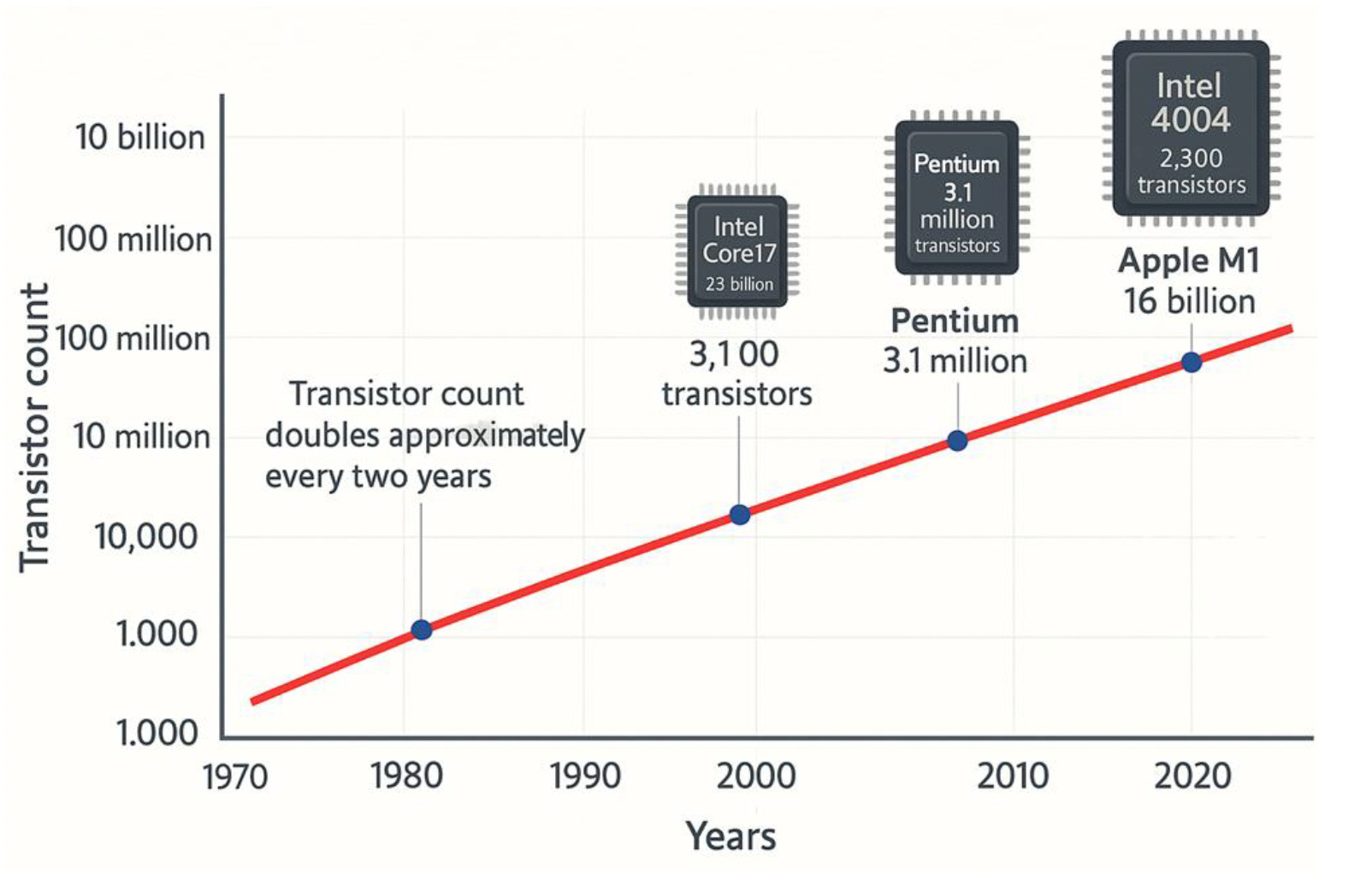
Exhibit 4: Historical Transistor Scaling Following Moore’s Law.Source: SemiWiki
History and Evolution of the Lithography Process
Lithography has evolved from early contact printing to projection-based DUV and immersion techniques through successive wavelength reductions, enabling continued transistor scaling and higher manufacturing precision
The evolution of lithography reflects the broader progression of the semiconductor industry. Initial lithographic techniques in the 1950s and early 1960s were based on contact printing and proximity printing, in which masks were placed in direct or near-direct contact with wafers. These methods were suitable for early micron-scale devices but quickly reached physical and contamination-related limitations. The advent of projection lithography in the early to mid-1970s, where a reduction lens projected the mask image onto the wafer without physical contact, represented a transformative shift, enabling better pattern fidelity and higher throughput. Subsequent innovation focused largely on decreasing exposure wavelengths: mercury-vapor lamp–based g-line (436 nanometers) became widespread in the late 1970s, followed by i-line (365 nanometers) in the mid-1980s. The industry then transitioned to deep ultraviolet (DUV) lithography at 248 nanometers using krypton fluoride (KrF) excimer lasers in the early 1990s, and 193 nanometers using argon fluoride (ArF) excimer lasers in the late 1990s. As the theoretical resolution limits of 193-nanometer exposure approached, the industry extended the technique through immersion lithography, introduced commercially around 2004–2005, in which the space between the projection lens and wafer was filled with ultrapure water to increase numerical aperture and improve resolution effectively.
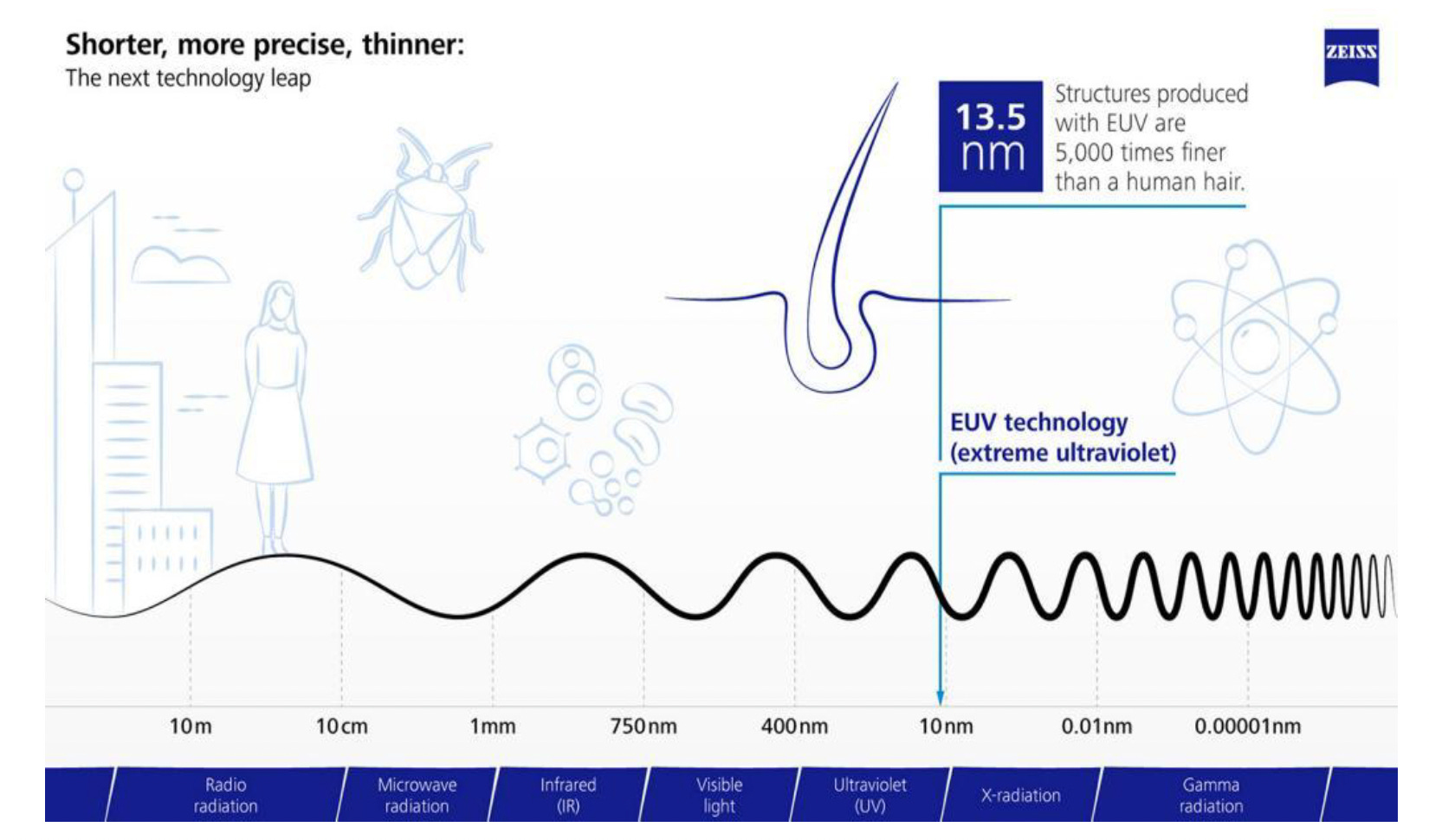
Exhibit 5: Extreme Ultraviolet (13.5 nm) Compared With the Broader Electromagnetic Spectrum. Source: ZEISS
The culmination of multi-decade optical engineering efforts was the development of extreme ultraviolet (EUV) lithography at 13.5 nanometers, whose first research breakthroughs emerged in the late 1990s, first lab-level tools appeared in the mid-2000s, and high-volume manufacturing finally arrived in 2019, enabling patterning below the 7-nanometer node and becoming essential for advanced logic and memory manufacturing. Each reduction in lithography wavelength correspondingly enabled smaller feature sizes, dropping from the micron scale in the 1980s to well below 100 nanometers by the early 2000s.
This progression culminated in EUV lithography at 13.5 nm, where wavelength, numerical aperture, and process repetition make lithography the defining bottleneck in advanced semiconductor manufacturing
At its core, lithography is governed by the Rayleigh resolution criterion, which states that the minimum feature size achievable on a wafer is proportional to the exposure wavelength and inversely proportional to the numerical aperture (NA) of the optical system. Achieving smaller transistors, therefore, requires either a shorter wavelength, a larger numerical aperture, or sophisticated computational corrections.
Modern lithography is an integrated sequence involving spin-coating a photoresist layer, exposing it through a projection system, thermally treating the exposed resist to catalyze chemical changes, developing the resist to reveal the patterned regions, etching those patterns into underlying layers, and finally stripping the resist to prepare for subsequent processing steps. Advanced chips require this sequence to be repeated hundreds of times, making lithography an operational bottleneck in semiconductor fabrication.
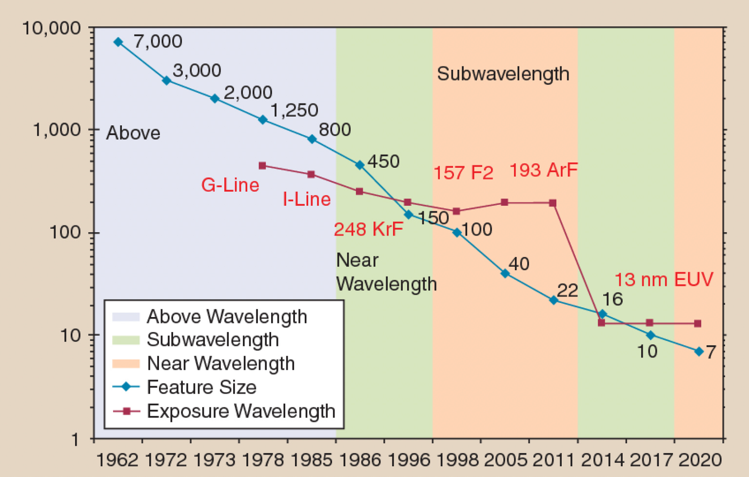
Exhibit 6: Evolution of Lithography Wavelengths and Feature Sizes (1980–2020). Source: SemanticScholar
Because physical optics alone is insufficient at today’s dimensions, computational lithography has become indispensable. Optical proximity correction (OPC), which adjusts mask shapes to compensate for optical distortions, and inverse lithography technology (ILT), which mathematically determines the optimal mask pattern for a desired wafer outcome, help counteract diffraction and process nonuniformities. These techniques rely on extremely large model-based simulations that must run on high-performance computing infrastructure, often involving graphics processing unit (GPU) acceleration. ASML’s acquisition of Brion Technology has positioned it as a leader in these computational workflows, turning lithography into an increasingly software-intensive domain.
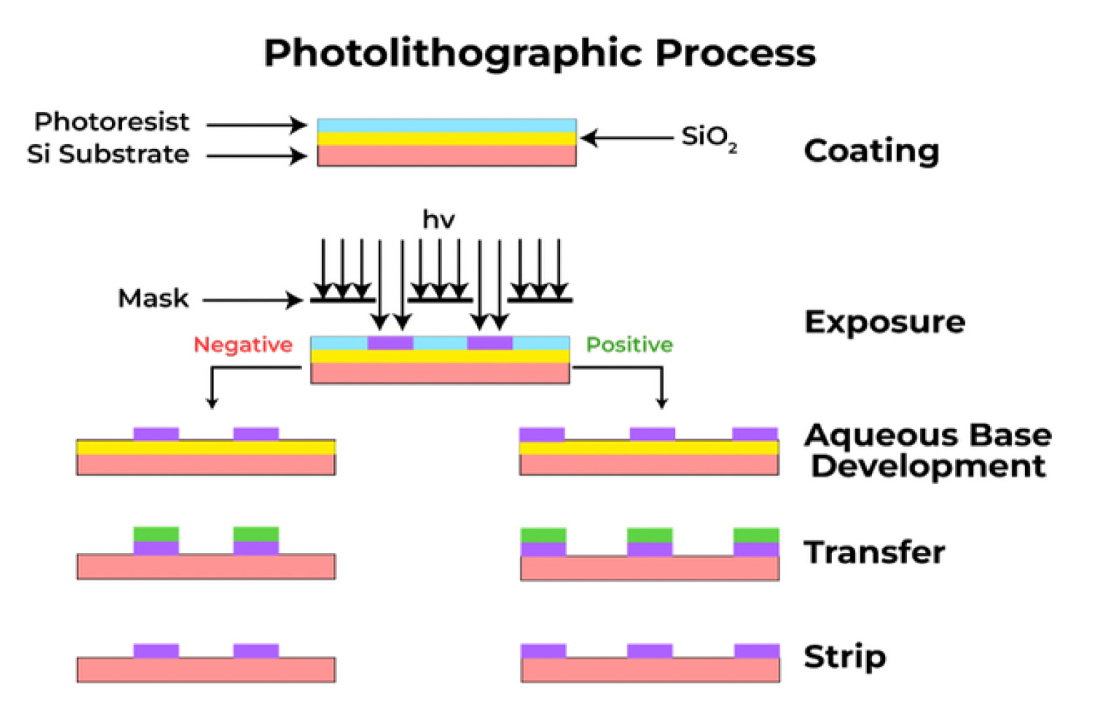
Exhibit 7: Overview of the Photolithography Process. Source: GeekforGeeks
How DUV and EUV Lithography Shape Semiconductor Patterning Complexity, Performance, and Cost at Advanced Nodes?
As physical and computational limits become tightly intertwined at advanced nodes, understanding how different wavelengths interact with the resist becomes essential to managing pattern fidelity, defects, and stochastic variability. The key difference between Deep Ultraviolet (DUV) and Extreme Ultraviolet (EUV) lithography is not only wavelength but also how energy interacts with the photoresist. DUV photons (248–193 nm, ~5–6.4 eV) directly activate the photoacid generator (PAG), producing predictable, localized chemical reactions. EUV photons (13.5 nm, ~92 eV), however, generate highly energetic electrons that release many low-energy secondary electrons (<10 eV). These secondary electrons drive most of the resist chemistry and spread energy non-uniformly, introducing stochastic variability such as line-edge roughness and pattern blur. This fundamental difference explains why EUV demands new resist materials, different process controls, and exhibits higher sensitivity to randomness at advanced nodes.
Deep ultraviolet (DUV) lithography remains a core component of semiconductor manufacturing, spanning i-line (365 nm), KrF (248 nm), and ArF (193 nm) technologies, including both dry and immersion configurations. While EUV is increasingly adopted at the most advanced nodes, DUV continues to account for a substantial share of lithography spending and unit volumes due to its cost efficiency, high throughput, and broad applicability across mature logic, memory, specialty devices, and advanced packaging. ArF delivers superior resolution within DUV methods and remains critical for patterning steps that do not yet require EUV. Demand is supported by growth in data-intensive applications such as 4K/8K video, online gaming, and AR/VR. The scale of deployment is evident in China, where ASML has installed a large base of DUV lithography and metrology systems to support expanding domestic semiconductor production. KrF lithography, operating at a 248 nm wavelength, remains widely used in mature logic, memory, and specialty applications where throughput, reliability, and cost of ownership are prioritized. Ongoing improvements in productivity and overlay accuracy have extended the economic relevance of KrF systems, particularly for high-volume manufacturing on 300 mm wafers. i-line lithography continues to serve applications that do not require the resolution of shorter-wavelength technologies. Advances in resolution and field size have expanded its role in back-end processes and advanced packaging, including 3D integration and chiplet-based architectures, where large exposure areas and cost efficiency are critical. ArF immersion lithography represents the most advanced DUV platform and remains essential for critical-layer patterning at advanced but pre-EUV nodes. Continued improvements in throughput and overlay accuracy have allowed ArF immersion to remain competitive, particularly in multi-patterning schemes that extend DUV at advanced nodes.
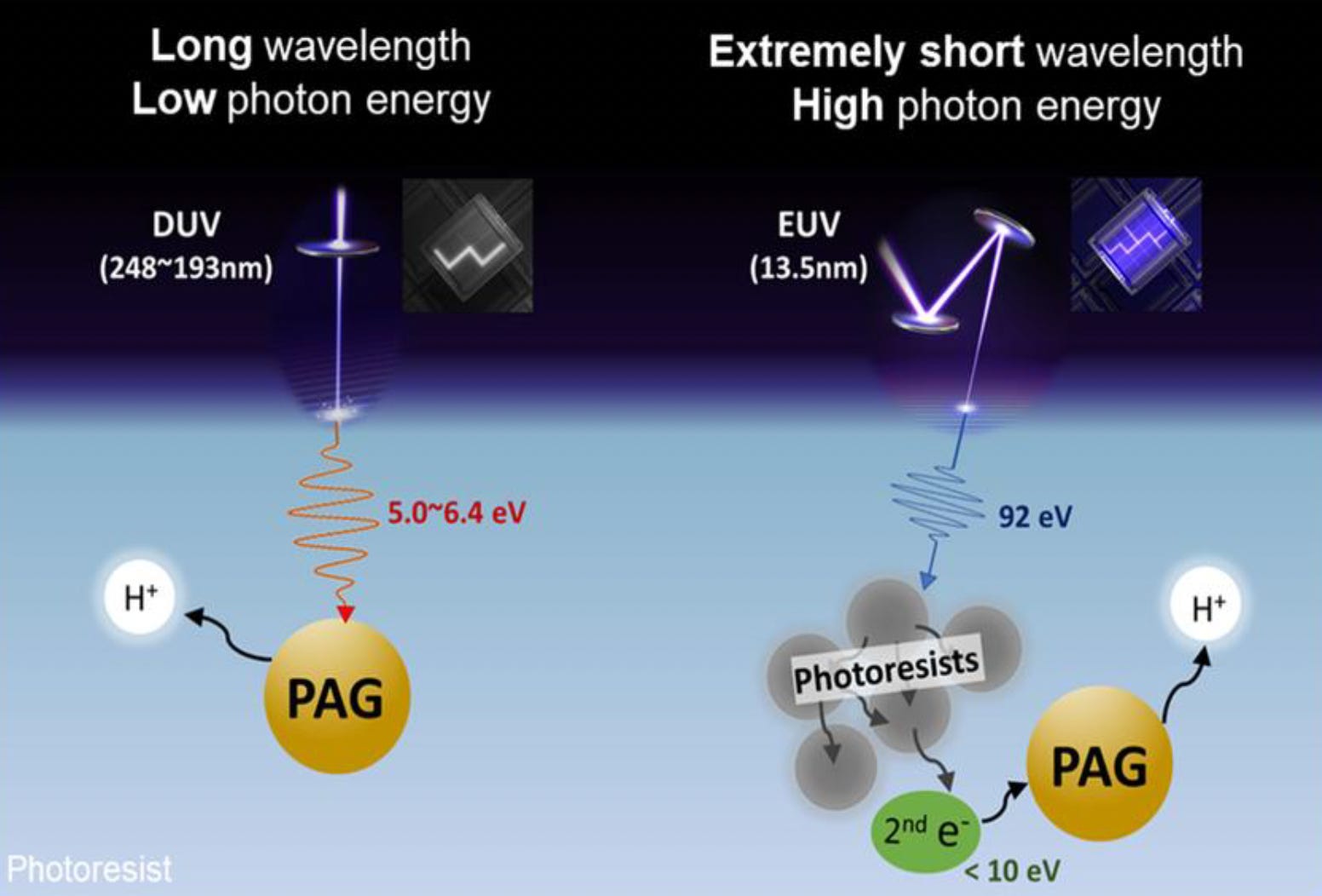
Exhibit 8: Comparison of DUV and EUV Photon-Resist Interaction Mechanisms. Source: Ji Young Park et al., 2023
EUV lithography is the most advanced patterning technology in high-volume manufacturing, enabling single-exposure scaling beyond DUV at advanced nodes while introducing significant engineering complexity
EUV lithography represents the most advanced and complex patterning technology deployed in high-volume semiconductor manufacturing today, enabling feature scaling that is no longer achievable with conventional DUV approaches. By operating at a much shorter wavelength, EUV allows many critical layers to be patterned in a single exposure, materially simplifying process flows at advanced nodes. While transformative, it introduces a host of new engineering challenges. Unlike DUV systems, which use transmissive quartz masks, EUV lithography uses reflective masks composed of multilayer molybdenum–silicon mirror stacks deposited with atomic-scale precision. Defects on or within these layers can translate into patterning errors on the wafer and are difficult to detect or repair. To protect masks from particle contamination, EUV systems use pellicles (ultra-thin, high-transmission membranes suspended over the mask), which must withstand extreme thermal loading from EUV exposure despite being only tens of nanometers thick. The EUV light source itself is one of the most complex subsystems in any manufacturing environment. It is based on laser-produced plasma (LPP) technology, in which droplets of molten tin are struck by a high-energy carbon dioxide (CO₂) laser to generate EUV radiation at 13.5 nanometers. This radiation is then collected and shaped by a series of specialized mirrors. Scaling EUV throughput requires higher source power, improved collector mirror efficiency, and advanced thermal management, all of which remain ongoing engineering challenges. ASML’s acquisition of Cymer in 2013 was instrumental in accelerating EUV development, bringing the critical laser-produced plasma light source in-house and enabling tighter integration of source power, dose stability, and collector protection technologies.
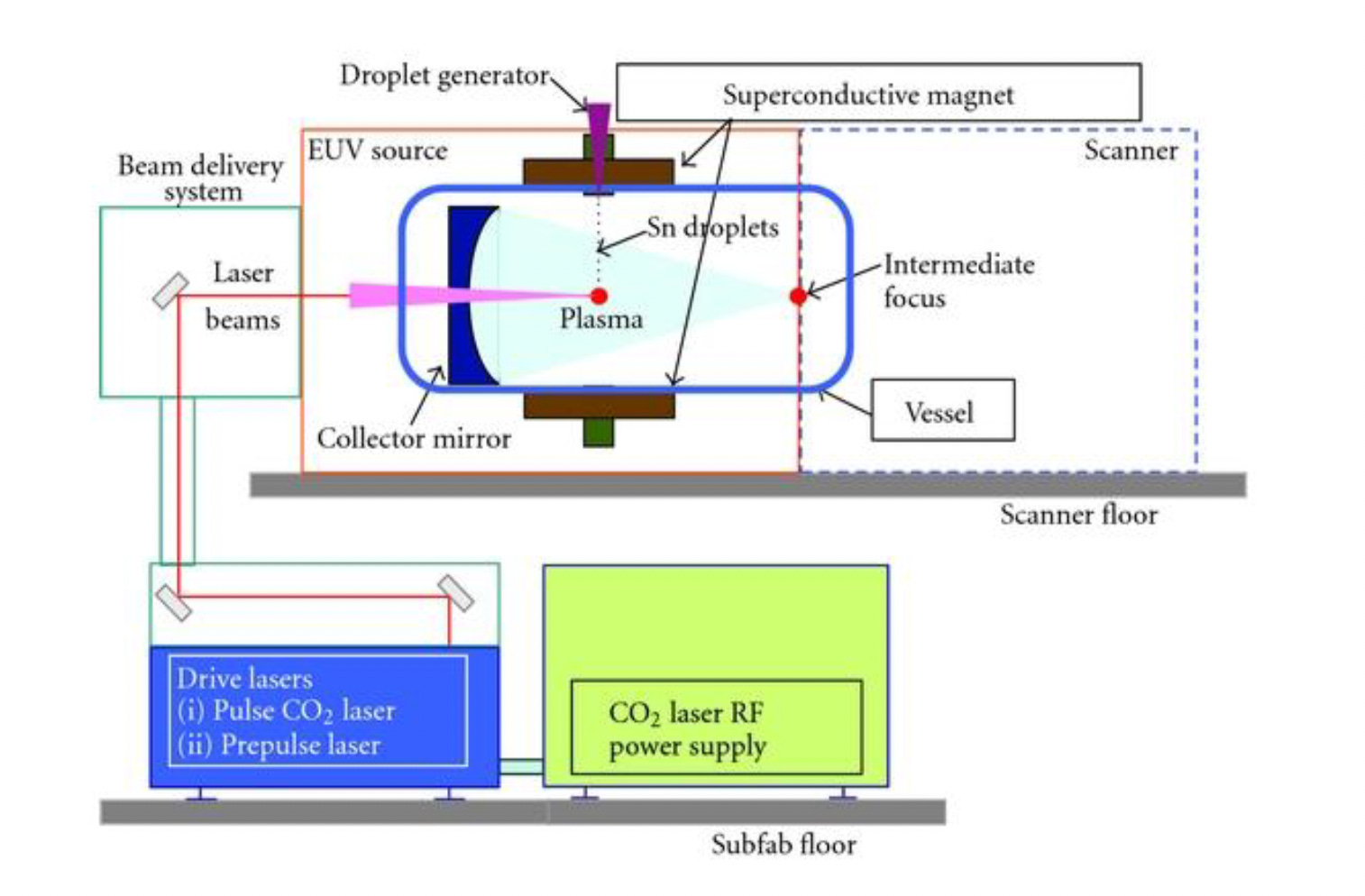
Exhibit 9: EUV Light Generation Using Tin Droplets and CO₂ Laser Drive Systems. Source: Wiley
The acceleration of EUV adoption has been supported by close collaboration between leading semiconductor manufacturers and equipment vendors to address throughput, defectivity, and stochastic variability challenges. Joint development programs between chipmakers and lithography suppliers have played a critical role in stabilizing EUV processes and accelerating readiness for next-generation nodes. These collaborations signal that EUV has moved beyond isolated tool deployment toward ecosystem-level optimization, solidifying its role as the industry’s primary scaling mechanism.
The optical system within modern lithography equipment is another engineering marvel. The EUV projection optics, manufactured exclusively by Carl Zeiss Semiconductor Manufacturing Technology (Carl Zeiss SMT), consist of multiple reflective mirrors, each with surface irregularities measured in fractions of a nanometer, operating in an ultra-high vacuum environment. These optics, along with the wafer and reticle stages, require exquisite mechanical and thermal stability. Wafer stages accelerate at more than ten times the force of gravity (10 g) while maintaining nanometer-level positioning accuracy. To achieve this stability, lithography systems employ advanced vibration isolation platforms, precision thermal compensation mechanisms, and real-time feedback control loops.
Before EUV lithography reached maturity, semiconductor manufacturers relied heavily on multi-patterning techniques such as double patterning (DP), quadruple patterning (QP), and self-aligned double patterning (SADP) to extend the useful life of 193-nanometer DUV exposure. Although effective, these techniques dramatically increased process steps, cycle time, defect risk, and production cost. EUV lithography streamlines these flows by enabling many critical layers to be patterned in a single exposure, offering both technical and economic benefits. Nevertheless, DUV lithography also remains indispensable for non-critical layers, benefiting from higher throughput and lower operational cost, and ensuring sustained demand for both DUV and EUV systems.
High-NA EUV extends optical lithography scaling to the 2-nanometer node and beyond by boosting numerical aperture to 0.55, materially improving resolution while increasing system complexity and process requirements
Exhibit 10: EUV Lithography Optics. Source: ZEISS
High NA EUV as the Next Scaling Inflection Point for Sub-2 Nanometer Semiconductor Manufacturing
High-numerical-aperture EUV (High-NA EUV) represents the next phase of optical lithography scaling and is critical for enabling patterning at the 2-nanometer node and beyond. By increasing the numerical aperture to 0.55 from 0.33 in current EUV systems, High-NA delivers a nearly 70 percent improvement in resolution, enabling tighter pitches and better control of line-edge and line-width roughness. The redesigned optical architecture employs anamorphic imaging, which halves the exposure field size and necessitates additional exposures or stitching strategies that can impact throughput, while also imposing more stringent requirements on photoresist sensitivity, stochastic defect control, and mask architecture.
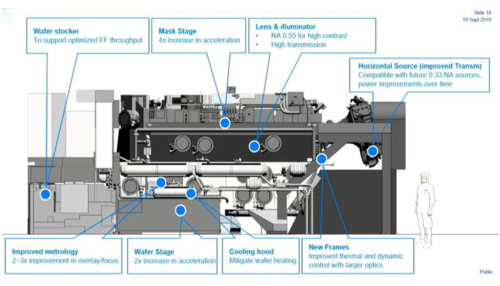
Exhibit 11: ASML HIGH-NA EUV System Architecture. Source: Company Filings
From an economic perspective, lithography is the most capital-intensive, throughput-defining, and technologically complex segment of the semiconductor manufacturing process. Tool productivity is measured in wafers per hour (WPH), uptime reliability, overlay performance, and defect control, with even marginal improvements yielding substantial increases in fab capacity and cost efficiency. As semiconductor technology scales to more advanced nodes, lithography accounts for an increasing proportion of total wafer fabrication costs, highlighting its growing economic weight within the semiconductor value chain and strengthening the strategic significance of companies like ASML that operate at the leading edge of lithographic innovation.
ASML Product Portfolio and Integrated Revenue Model Across the Semiconductor Lithography Value Chain
ASML’s business is built around the development, manufacture, and servicing of advanced lithography systems that are critical to semiconductor fabrication. In 2024, ASML reported total net sales of approximately €28.3 billion (accounting for approximately 90% of the overall market for advanced lithography machines), reflecting its pivotal role across leading-edge logic, advanced memory, and specialty semiconductor manufacturing. The company’s product portfolio spans conventional EUV (including next-generation High-NA EUV lithography), DUV immersion and DUV dry platforms, refurbished lithography systems, as well as metrology, inspection, and computational lithography software, all supported by a large and recurring Installed Base Management business. Together, these offerings form a deeply integrated revenue model that combines high-value capital equipment sales with lifecycle services, upgrades, refurbished tool redeployments, and software-driven optimization, allowing ASML to participate across the full patterning workflow and multiple technology generations.
ASML’s revenue base is concentrated among a small group of advanced semiconductor manufacturers, including leading foundries and IDMs. While such concentration would typically raise risk concerns, in ASML’s case, it reflects mutual dependence rather than buyer leverage. Customers depend on ASML to execute their technology roadmaps, while ASML relies on these customers to absorb the cost and complexity of next-generation tools. This alignment fosters long-term partnerships, early access programs, and shared development risk.
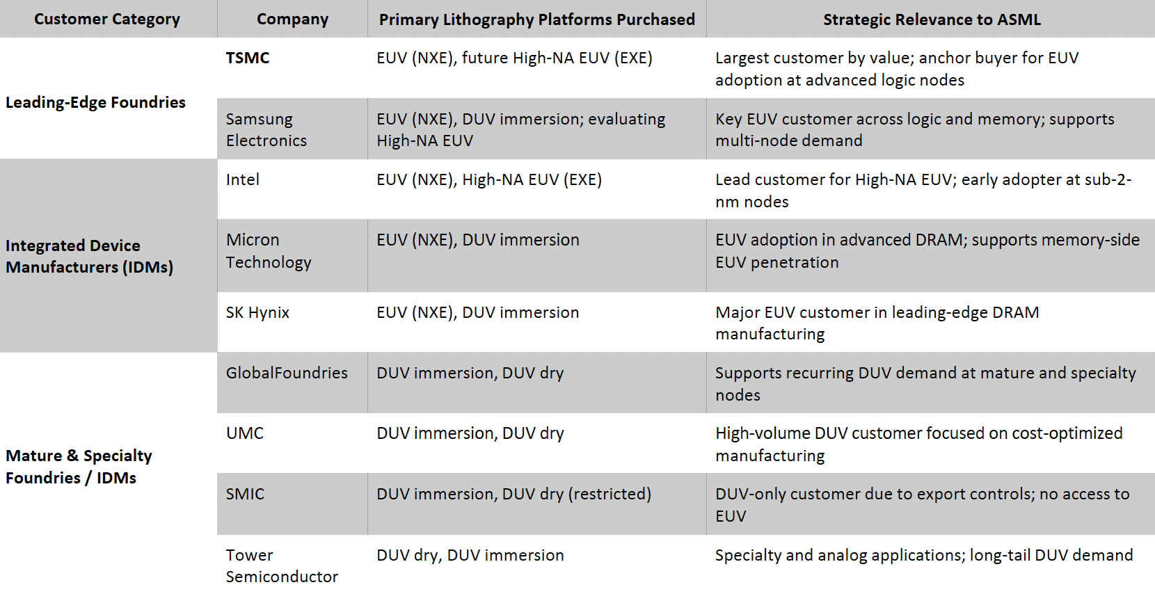
Exhibit 12: ASML’s Notable Customer Base Across Lithography Platforms. Source: Business Deep Dives’ Research.
While fabless companies (which design and sell semiconductor chips but do not own the costly manufacturing fabs, instead outsourcing production to specialized foundries like TSMC) do not purchase lithography systems directly, they are economically dependent on ASML through their reliance on foundries equipped with EUV and advanced DUV tools. Leading fabless firms, such as NVIDIA, Apple, AMD, Qualcomm, and Broadcom, ultimately depend on manufacturing capacity at foundries like TSMC and Samsung, which is enabled by ASML’s lithography platforms. This indirect reliance extends ASML’s influence well beyond its direct customer base, embedding the company structurally across the entire semiconductor value chain. In this context, ASML’s products and services constitute the core enabling layer of advanced semiconductor manufacturing across the global value chain. To better understand ASML’s central role within the semiconductor value chain, the following section provides an overview of the company’s product and services portfolio.
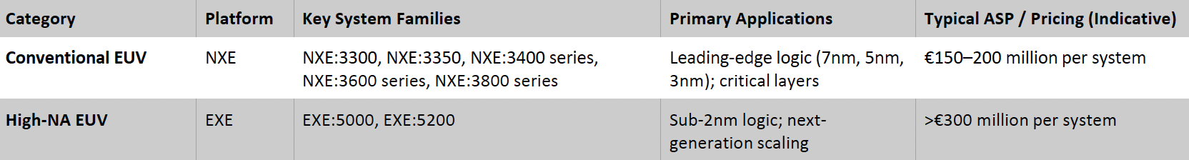
Conventional EUV Lithography Systems (NXE Platform)
Conventional EUV lithography systems are marketed under ASML’s NXE platform and represent the most economically significant advanced-lithography category in the portfolio. The NXE family comprises multiple generations of EUV scanners that enabled both the initial insertion and subsequent scaling of EUV into high-volume manufacturing. These include early platforms such as NXE:3300 and NXE:3350, followed by the production-scale NXE:3400 series, the productivity-enhanced NXE:3600 series, and the current NXE:3800 series, which serves as the primary workhorse for leading-edge 3-nanometer logic manufacturing.
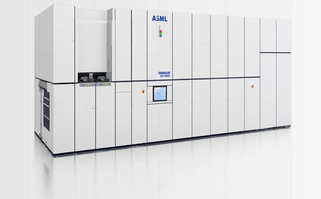
Exhibit 13: TWINSCAN NXE:3800E EUV System. Source: Company Filings
Operating at a wavelength of 13.5 nanometers, NXE systems are used for the most critical patterning layers where alternative lithography approaches are no longer viable. Continuous improvements in source power, throughput, overlay accuracy, and system availability have enabled EUV to transition from selective layer insertion to broad multi-layer deployment. From an economic standpoint, EUV tools command exceptionally high average selling prices, typically in the range of €150–200 million per system, resulting in a disproportionate revenue contribution relative to shipment volumes. In Q3 2025, ASML generated €2.1 billion in EUV system revenue, accounting for approximately 38% of total net system sales (€5.6 billion) and around 28% of total net sales (€7.5 billion), despite delivering only 9 EUV tools out of 72 lithography systems shipped during the quarter. This disproportionate revenue contribution emphasizes the exceptionally high value density of EUV platforms validating ASML’s structural pricing power within advanced lithography. Beyond initial system shipments, the NXE platform anchors long-term customer relationships and drives substantial follow-on revenue through upgrades, spare parts, and service contracts, emphasizing its importance to both top-line growth and margin expansion.
High-Numerical-Aperture EUV Lithography Systems (EXE Platform)
High-NA EUV lithography systems represent ASML’s next major technology inflection and are delivered under the EXE platform, most notably through the EXE:5000 and the follow-on EXE:5200 series. These systems increase numerical aperture from 0.33 to 0.55, enabling materially higher resolution and extending optical lithography scaling into the sub-2-nanometer regime. Compared with current NXE EUV tools, the EXE platform introduces a fundamentally new architecture, including anamorphic optics, larger reticle formats, redesigned wafer stages, and substantially higher system complexity, reflecting the demands of next-generation patterning.
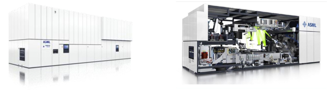
Exhibit 14: TWINSCAN EXE:5200B. Source: Company Filings
Although still in early commercial deployment, High-NA EUV systems are widely viewed as the next major value driver in lithography. These tools are expected to command average selling prices in the €300–350 million range per system, reflecting their unprecedented technical complexity and strategic importance at the leading edge of technology. Initial shipments have been limited to a small group of advanced logic manufacturers, with Intel taking the lead in early adoption, while TSMC and Samsung are evaluating deployment timing as part of their sub-2-nanometer roadmaps. While near-term revenue contribution remains modest relative to NXE systems, High-NA EUV is positioned as a structural growth engine later in the decade, supported by long-duration service attachment, high switching costs, and deep integration into customers’ most advanced process flows.
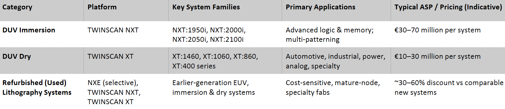
DUV Immersion Lithography Systems (TWINSCAN NXT Platform)
DUV immersion lithography systems are marketed under the TWINSCAN NXT platform and remain essential across advanced logic and memory manufacturing. The NXT platform includes systems such as the NXT:1950i, NXT:2000i, NXT:2050i, and NXT:2100i, which operate at a 193-nanometer wavelength using immersion technology. These tools are widely deployed for critical layers where EUV is either unnecessary or less cost-effective, particularly in memory and multi-patterning-intensive process flows.
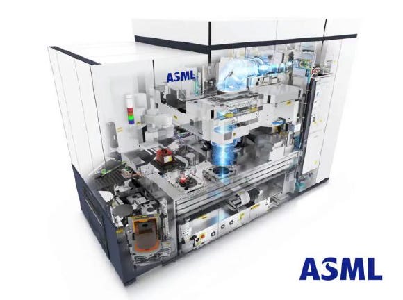
Exhibit 15: TWINSCAN NXT:2000i. Source: Company Filings
DUV immersion systems typically command average selling prices of approximately €30–70 million per system, offering an attractive balance between resolution capability and capital efficiency. Despite the structural shift toward EUV at leading-edge logic nodes, immersion tools continue to play a central role in DRAM and NAND manufacturing and provide meaningful diversification within ASML’s system revenue. In Q3 2025, DUV immersion systems collectively accounted for 52% of ASML’s approximately €5.5–5.6 billion in system sales, with 38 immersion tools shipped out of a total of 72 lithography systems delivered during the quarter, highlighting the continued volume dominance and revenue relevance of advanced DUV platforms alongside EUV within ASML’s system mix.
DUV Dry Lithography Systems (TWINSCAN XT Platform)
DUV dry lithography systems are delivered through the TWINSCAN XT platform and serve mature-node, specialty, and cost-sensitive semiconductor applications. This platform encompasses a wide range of systems, including the XT:1460, XT:1060, XT:860, and XT:400 series, which are widely used in automotive electronics, industrial semiconductors, power devices, analog ICs, and selected memory layers. These tools prioritize throughput, stability, and long operational lifetimes rather than extreme resolution.
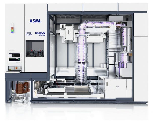
Exhibit 16: TWINSCAN XT:400M (R). Source: Company Filings
DUV dry tools typically command average selling prices in the range of €10–30 million per system, reflecting lower complexity but long useful lives. From a business perspective, the XT platform provides exposure to end markets characterized by longer product cycles and more stable capital-spending behavior, while supporting a large installed base that generates recurring service and upgrade revenue over extended periods.
Refurbished Lithography Systems
ASML also offers refurbished lithography systems as part of its lifecycle-driven portfolio, enabling the redeployment of proven tools into cost-sensitive and mature-node applications. These systems are primarily sourced from the TWINSCAN NXT (DUV immersion) and TWINSCAN XT (DUV dry) platforms, with selective redeployments of earlier-generation NXE EUV systems following reconfiguration and targeted upgrades. Refurbished tools are typically priced at a 30–60% discount to comparable new systems, depending on system configuration and the scope of enhancements. Offered through ASML’s installed base management organization, refurbished systems extend tool lifecycles, address sustained demand at non-leading-edge nodes, and further strengthen the recurring, installed-base-driven nature of the company’s revenue model.
Source: Company Filings, Business Deep Dives Research
Metrology Systems (YieldStar Platform)
ASML’s metrology portfolio is delivered primarily through the YieldStar platform, which provides optical process-control solutions tightly integrated with the company’s lithography systems. YieldStar tools measure critical dimensions, overlay accuracy, and focus performance, enabling fabs to detect and correct deviations in real time. Key systems include the YieldStar 385, widely used in DUV-based flows, and the YieldStar 1385, optimized for EUV environments where tolerances are significantly tighter.
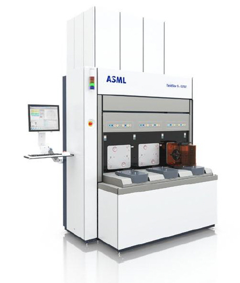
Exhibit 18: Yieldstar 1385. Source: Company Filings
YieldStar systems typically carry average selling prices of approximately €5–15 million per tool. While metrology represents a smaller share of total revenue compared with lithography systems, it plays a critical role in yield ramp, process stability, and cost control at advanced nodes, enhancing overall value capture per fab.
Inspection Systems (HMI E-Beam Platform)
Inspection capabilities are largely derived from ASML’s HMI e-beam platform, which focuses on advanced wafer and mask inspection. These systems are designed to detect extremely small defects that are increasingly difficult to identify using optical inspection, particularly in EUV and future High-NA EUV process flows. E-beam inspection tools typically command average selling prices ranging from a few million euros up to €20 million per system.
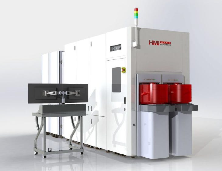
Exhibit 19: HMI eScan 600. Source: Company Filings
Although inspection systems represent a modest portion of ASML’s overall revenue, they play a critical enabling role during process development and early production ramps, where identifying stochastic and yield-limiting defects is essential. Their integration into ASML’s broader ecosystem further deepens customer reliance across multiple stages of the patterning process.
Computational Lithography and Software (Brion Platform)
ASML’s computational lithography offerings, delivered through the Brion platform, form a central pillar of its holistic lithography strategy. These software solutions use advanced modeling and simulation to optimize mask design, illumination settings, and exposure conditions, compensating for optical distortions, process variability, and stochastic effects inherent in EUV lithography. As hardware-only scaling becomes increasingly difficult, computational lithography has become essential to sustaining pattern fidelity at advanced nodes.
While software contributes a relatively small share of revenue in absolute terms, it is high-margin and recurring, and it materially increases the economic return on ASML’s hardware systems by extending performance limits without additional capital equipment.
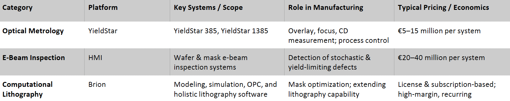
Exhibit 20: Metrology, Inspection, and Computational Lithography Segments. Source: Company Filings, Business Deep Dives’ Research.
Installed Base Management and Services
Installed Base Management encompasses system installation, maintenance, spare parts, upgrades, productivity enhancements, and refurbished-system redeployments across ASML’s global installed base. This segment benefits directly from the expanding installed base of EUV and DUV systems, delivering structurally higher margins and more predictable cash flows than new system sales, smoothing the cyclicality inherent in semiconductor capital-equipment demand. In Q3 2025, Installed base management generated approximately €1.96 billion in revenue out of total quarterly net sales of €7.5 billion, or about a quarter of total sales, highlighting the scale and stabilizing influence of services within ASML’s business model.
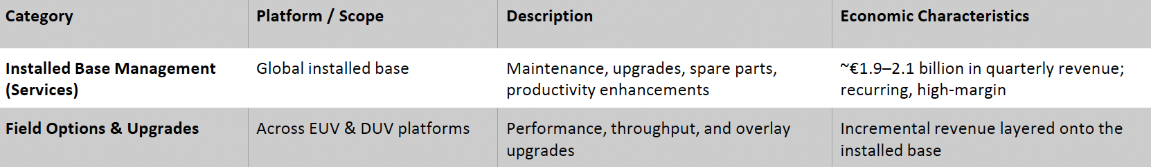
Exhibit 21: Installed Base Management Segments. Source: Company Filings, Business Deep Dives’ Research.
Taken together, ASML’s products and services portfolio reflects a uniquely integrated approach to semiconductor manufacturing that extends well beyond the sale of new lithography equipment. By spanning EUV and High-NA EUV systems, DUV immersion and dry platforms, refurbished lithography systems, metrology, inspection, computational lithography software, and comprehensive lifecycle services, ASML positions itself at every critical stage of the patterning process and across the full equipment lifecycle. This breadth enables value capture across leading-edge transitions as well as high-volume and specialty markets, enhances revenue visibility, supports structurally strong margins, and embeds ASML deeply within customer manufacturing workflows, corroborating durable growth, pricing power, and long-term strategic relevance.
ASML operates at the most complex and capital-intensive chokepoint of semiconductor manufacturing, where lithography commands a growing share of WFE spending and is expected to expand from ~€25–26 billion today to over €40 billion by the end of the decade
The Patterning Monopoly Controlling the Global Semiconductor Value Chain
ASML operates in one of the most technologically complex and capital-intensive segments of the semiconductor equipment industry, photolithography, where barriers to entry are exceptionally high, and competition varies sharply by technology tier. Independent industry research estimates the global semiconductor lithography equipment market at approximately €25-26 billion in the mid-2020s, with projections indicating expansion to over €38-40 billion by the end of the decade, implying a high-single-digit CAGR. Lithography sits at the core of semiconductor manufacturing economics, acting as both the most technologically complex and the most capital-intensive step in the wafer fabrication process. At advanced logic and memory nodes, lithography alone accounts for a disproportionate share of total fab capital expenditure, reflecting the extreme precision, system integration, and process control required to pattern features at atomic-scale dimensions. This growth reflects the rising complexity of patterning as technology nodes advance and lithography accounts for an increasing share of overall wafer fabrication equipment (WFE) spending.
Crucially, this market expansion is not evenly distributed across lithography technologies. A disproportionate share of incremental spending is concentrated in advanced logic and memory manufacturing, where tighter geometries, yield sensitivity, and overlay requirements necessitate the use of EUV lithography. Within this fastest-growing and most value-intensive segment, ASML’s competitive position remains structurally dominant. At leading-edge logic nodes, ASML is the sole commercial supplier of EUV systems, which are indispensable for manufacturing at 7-nanometer and below, and no competitor has successfully commercialized an EUV platform at production scale due to the extraordinary integration challenges across optics, light sources, vacuum systems, materials, and software. The lithography equipment industry is therefore characterized by extreme concentration, with ASML estimated to control approximately 80–85% of global lithography revenue, including a 100% share in EUV and over 90% share in the most economically critical immersion-based DUV segment. Competitive pressure elsewhere in DUV is uneven and largely confined to lower-value layers that are less sensitive to wafer cost and yield, limiting its impact on ASML’s overall pricing power and strategic relevance as demand increasingly tilts toward EUV-driven manufacturing.
The remainder of the lithography market is primarily served by Nikon and Canon, both of which have gradually shifted their focus toward mature-node and specialty segments over the past decade. Nikon maintains a limited presence in ArF immersion and KrF tools, primarily focusing on trailing-edge logic and select memory applications, while Canon has concentrated its semiconductor exposure on i-line systems for mature nodes and image sensor manufacturing. Neither company maintains a credible roadmap for next-generation optical lithography beyond conventional DUV, and neither participates in EUV development.
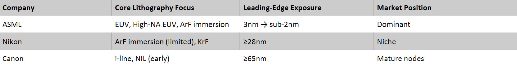
Exhibit 22: Lithography Competitive Positioning. Source: Business Deep Dives’ Research
Other players participate only marginally, primarily in niche exposure or specialty lithography tools, and do not significantly influence the competitive or economic structure of the market. As a result, industry growth and profit pools are overwhelmingly captured by ASML, while competitors remain structurally underexposed to the segments driving long-term value creation. Beyond external competitors, ASML’s dominance is fortified by the scale and sophistication of its supplier ecosystem. In 2024, ASML operated with approximately 5,150 suppliers globally across Europe, the United States, and Asia, reflecting the extreme specialization and co-development required to manufacture advanced lithography systems. Rather than commoditizing inputs, this supplier base functions as an extension of ASML’s technological advantage, embedding proprietary processes, long qualification cycles, and high coordination costs that materially raise barriers to entry for any potential challenger.
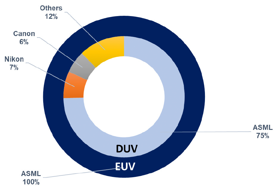
Exhibit 23: Global DUV and EUV Lithography Equipment Market Share by Supplier (2024). Source: Industry Estimates, Business Deep Dives Research
The competitive dynamic differs fundamentally from other Wafer fabrication equipment (WFE) categories, such as deposition, etch, or metrology, where multiple vendors compete across overlapping product portfolios, and customers can substitute between tool vendors within a given process step. In lithography, the market has bifurcated into a monopolistic leading-edge segment controlled by ASML and a fragmented mature-node segment where Nikon and Canon operate with structurally lower margins and limited growth prospects. Within the broader WFE ecosystem, ASML does not face direct product competition from diversified equipment suppliers such as Applied Materials, Lam Research, or Tokyo Electron, as none offer lithography systems or credible substitutes for EUV. However, these companies compete indirectly with ASML for customer capital allocation within semiconductor fabs. Semiconductor manufacturers operate under finite capital budgets, and investment decisions involve trade-offs across lithography, deposition, etch, inspection, and packaging to optimize overall yield, cost, and time-to-market.
In periods of tight capex or technology transitions, customers may sequence or defer lithography purchases in favor of incremental process investments elsewhere in the fab, particularly at mature nodes. Despite this budget-level competition, lithography, especially EUV, remains the primary enabler of node shrinks, limiting customers’ ability to structurally underinvest without compromising roadmap execution. Reflecting this dynamic, ASML’s financial profile has increasingly converged with, and in some cases surpassed, that of the largest WFE peers. By FY2024, ASML had emerged as one of the top two global WFE suppliers by revenue, while maintaining structurally higher gross margins. This margin profile reflects monopoly economics driven by technological indispensability, rather than scale-driven volume leverage typical of multi-vendor WFE categories, substantiating ASML’s unique competitive position within the semiconductor capital equipment landscape.
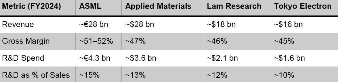
Exhibit 24: FY2024-25 WFE Vendor Comparison. Source: Business Deep Dives’ Research.
Competitive Moat: R&D, Vertical Integration, & Switching Costs
At the heart of ASML’s moat lies its exclusive mastery of EUV lithography. No alternative technology has demonstrated the ability to replicate EUV’s resolution, throughput, and overlay precision in high-volume manufacturing. By the end of 2025, ASML had installed over 200 EUV systems globally, with EUV adoption now standard across all leading-edge logic fabs and expanding into advanced DRAM layers. Each EUV system represents one of the most complex machines ever produced, incorporating tens of thousands of components, ultra-high vacuum chambers, and precision optics capable of reflecting EUV light with near-atomic accuracy. The technological hurdles involved are such that even well-capitalized industrial conglomerates would face decades-long development timelines to approach parity. Importantly, ASML’s EUV monopoly is not approaching saturation. Instead, it is entering a new phase of extension through the introduction of High-NA EUV. ASML began shipping the first High-NA EUV systems (EXE:5200 series) to early customers (Intel) in 2024, with pilot production underway during 2025 and broader volume deployment expected from 2026-27 onward. High-NA EUV does not reset ASML’s competitive position; rather, it deepens the existing moat. As customers transition to High-NA EUV, dependency on ASML intensifies, bolstering long-term pricing power and service revenue potential. ASML’s technology leadership is sustained by a level of R&D investment that no competitor can economically match. In FY2024, ASML invested approximately €4.3 billion in R&D (an increase of 8.1% over the previous year), with EUV and High-NA EUV programs spanning decades of coordinated engineering effort, equivalent to roughly 14-15% of revenue. This spending is overwhelmingly focused on lithography-specific challenges, including optics, light sources, metrology, computational lithography, and system integration. By contrast, Nikon’s semiconductor-related R&D spending has fallen below €0.5 billion annually, while Canon’s group-wide R&D budget, spread across imaging, office equipment, and healthcare, offers only limited focus on semiconductor lithography. The result is a widening R&D gap that compounds over time. Even if competitors were to increase spending meaningfully, the cumulative deficit relative to ASML would remain prohibitive.
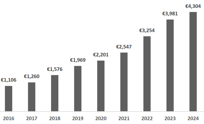
Exhibit 25: ASML Research and Development (R&D) Costs (in € million). Source: Company Filings, Business Deep Dives’ Research.
ASML’s competitive advantage extends well beyond its lithography hardware, resting on a tightly integrated ecosystem anchored by a vast intellectual property portfolio and exclusive strategic relationships. As of 2025, the company holds approximately 38,000 patents worldwide, encompassing lithography systems, optics, software, and process control technologies. This extensive patent base reflects decades of cumulative innovation, creating a dense layer of protection that is extremely difficult for competitors to replicate or circumvent.
In tandem, ASML has strengthened its competitive position through the deliberate internalization of several critical subsystems within the lithography stack. The acquisitions of Brion Technologies (computational lithography software), Cymer (EUV light sources), and HMI (e-beam inspection) have enabled ASML to vertically integrate capabilities that are essential to advanced patterning. This integration has reduced reliance on external suppliers, accelerated co-optimization across hardware, software, and process control, and further solidified ASML’s leadership across the lithography value chain. Each of these capabilities represented a former bottleneck in advanced lithography, and their integration has allowed ASML to control not only exposure hardware but also the modeling, photon generation, and defect-detection layers essential to yield and scaling. This vertical integration materially increases entry friction by eliminating external dependencies that competitors would need to replicate in parallel.
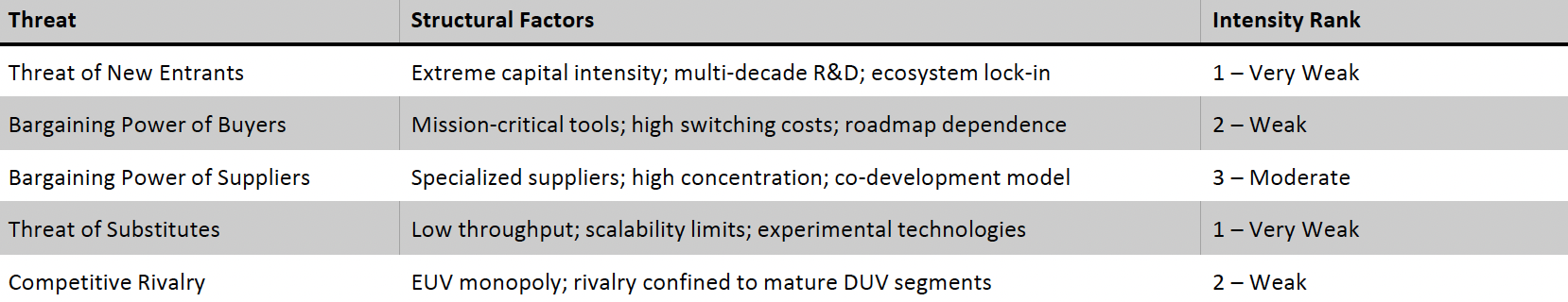
Exhibit 26: Analysis of the Lithography Equipment Industry Competition. Source: Business Deep Dives’ Research.
A key differentiator in ASML’s competitive profile is the degree of process lock-in and switching cost associated with lithography tools. Lithography systems are deeply embedded within customers’ process recipes, yield models, and fab workflows, and switching suppliers typically requires extensive re-qualification cycles that can extend 12-24 months. At advanced nodes, where yield excursions can have material financial consequences, and time-to-market is critical, customers are highly risk-averse, materially reducing the practical threat posed by alternative tools even where they exist in principle. By 2025, ASML had an installed base of thousands of DUV systems and more than 200 EUV systems globally. This installed base strengthens a growing services business, which now accounts for approximately 25% of ASML’s revenue. Service contracts provide recurring, high-margin cash flows and enable continuous performance upgrades, further embedding ASML within customer operations. The service flywheel also generates data and process insights that feed back into R&D, and further consolidates ASML’s technology leadership while accelerating learning curves.
Secular Demand Tailwinds Supporting Long-Term Growth in Advanced Lithography
The long-term outlook for lithography demand is shaped by several secular forces that collectively favor ASML. Foremost among these is the rapid growth of artificial intelligence (AI) and high-performance computing. AI accelerators and advanced CPUs require leading-edge process nodes to deliver performance and energy efficiency gains, driving sustained demand for EUV and, eventually, High-NA EUV systems. Importantly, AI workloads tend to increase lithography intensity per wafer, as advanced chips require more patterning layers and tighter overlay control. At the same time, while the pace of traditional Moore’s Law scaling has moderated, patterning complexity continues to rise. Even incremental node shrinks require disproportionately greater lithography precision, increasing the value of ASML’s tools. This dynamic has shifted lithography from a cost center to a strategic enabler, augmenting customer willingness to invest in advanced systems.
AI/ML as a Structural Demand Driver for Leading-Edge Lithography
The acceleration of artificial intelligence and machine learning workloads has emerged as one of the most powerful structural demand drivers for advanced semiconductor manufacturing, with outsized implications for lithography intensity and capital spending at the leading edge. Generative AI models, large-scale training clusters, and inference workloads are driving explosive growth in demand for high-performance computing silicon, including GPUs, dedicated AI accelerators, and advanced server CPUs. These devices are overwhelmingly manufactured on the most advanced logic nodes, 5 nm, 4 nm, 3 nm, and moving toward 2 nm, all of which are fundamentally dependent on EUV lithography.
Industry estimates indicate that AI-related chips accounted for more than US$120 billion of global semiconductor sales in 2024, representing roughly 20% of the total semiconductor market, with this share expected to expand further up to US$500 billion in 2028 as cloud service providers and hyperscalers continue to scale AI infrastructure. This demand profile has translated directly into robust fab investment at the cutting edge, with leading logic manufacturers such as TSMC, Samsung Electronics, and Intel consistently highlighting AI as a primary driver behind capacity expansion at 3 nm and upcoming 2 nm nodes.
For ASML, the relevance of this trend extends beyond simple wafer volume growth. Advanced AI accelerators are among the most lithography-intensive devices produced, requiring a higher number of critical patterning layers, tighter overlay tolerances, and increasingly complex multi-exposure schemes. As a result, lithography intensity, measured by lithography cost per wafer and number of lithography steps, rises materially at advanced nodes, amplifying demand for EUV tools and associated services. This dynamic ensures that ASML benefits disproportionately from AI-driven semiconductor growth relative to other WFE suppliers whose exposure is more evenly distributed across process steps.
However, a key downside risk to the current AI-led semiconductor upcycle is the possibility that AI-driven compute demand fails to generate sustainable economic returns, prompting hyperscalers to moderate capital spending. Although AI workloads represent a minority share of total semiconductor volumes, they account for a disproportionately large share of advanced-node wafer starts and leading-edge capital expenditure, particularly at ≤5 nm logic and advanced DRAM nodes. Any normalization in AI investment could therefore have a non-linear impact on equipment demand: a hypothetical 20–25% reduction in AI-driven wafer demand would likely translate into a disproportionately larger decline in leading-edge lithography demand, given that EUV and advanced ArF immersion tools carry the highest incremental capex per wafer and are most closely tied to node transitions. Under such conditions, customers could defer node migrations, extend tool utilization, and prioritize yield optimization over capacity expansion, leading to delayed EUV orders, slower backlog conversion, and heightened volatility in system sales for ASML, whose revenue mix has become increasingly concentrated in the most capital-intensive segments of the semiconductor manufacturing stack.
Long-term demand for advanced lithography is driven by AI-led leading-edge compute growth and policy-backed global fab expansion, both of which increase lithography intensity per wafer and structurally favor EUV and High-NA adoption
Geographic Fab Expansion Due to Policy-Led Capacity Buildout in the US, Europe, and Japan
Government-led semiconductor re-shoring initiatives across the United States, Europe, and Japan are driving hundreds of billions of dollars in committed fab capital expenditure through the end of the decade, creating a second structural demand pillar for advanced lithography alongside AI-driven compute growth. Critically, these programs are skewed toward advanced logic, memory, and advanced packaging, rather than mature-node capacity, resulting in elevated lithography intensity and high EUV tool density per fab, and directly reinforcing ASML’s strategic importance within the global semiconductor supply chain.
In the United States, the CHIPS and Science Act has catalyzed an estimated USD 200–250 billion of announced semiconductor investment through 2030, spanning leading-edge logic, memory, and advanced packaging. Major projects include TSMC’s Arizona fabs (>$65 bn committed), Intel’s multi-site build-out across Arizona and Ohio (>$100 bn potential investment) and continued advanced-node investment by Samsung Electronics in Texas. These facilities are anchored at 4 nm, 3 nm, and future 2 nm nodes, implying high EUV penetration per fab and sustained pull-through for DUV immersion and installed-base services during ramp and node migration.
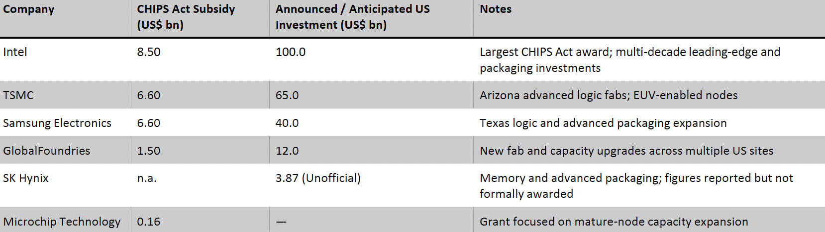
Exhibit 27: Overview of US Chip Subsidy Recipients and Amounts in US$ billion (2024-25). Source: Business Deep Dives’ Research.
Europe’s semiconductor strategy under the European Chips Act supports an estimated €100–120 billion of potential investment by 2030, with incentives skewed toward advanced logic, automotive, and specialty semiconductors rather than commodity mature nodes. While Europe’s absolute wafer starts remain lower than those in the US or Asia, the incremental capacity is disproportionately lithography-intensive, particularly in automotive and industrial applications. Flagship projects enabled by the European Chips Act now include the ESMC joint venture in Germany (involving TSMC, Bosch, Infineon, and NXP) planning over €10 billion in multi-node logic capacity with ~€5 billion in approved state aid, Infineon’s €4.46 billion Dresden fab expansion supported by €920 million in German state funding, STMicroelectronics’ €5 billion silicon carbide fab in Italy backed by ~€2 billion of state support, and a €3.2 billion advanced packaging facility in Novara secured with ~€1.3 billion of aid, collectively facilitating sustained demand for advanced DUV immersion and selective EUV systems despite lower overall wafer volumes.
Japan represents the most fiscally aggressive semiconductor support program globally on a GDP-adjusted basis, effectively functioning as a national CHIPS Act despite the absence of a single legislative label. Between FY2021 and FY2023, the Japanese government committed JPY 3.9 trillion (US$27 bn) (equivalent to ~0.7% of GDP) to semiconductor support, a higher share than comparable US or EU programs. In November 2024, this was followed by a JPY 10 trillion (US$64 bn) commitment through FY2030. Crucially, funding is highly concentrated at the company level, with roughly 40% of the capital cost of JASM’s (a joint venture between TSMC, Sony, and Denso) Kumamoto fab is government-subsidized, while approximately 20% of the capital required for mass production at Rapidus (a government-backed venture with a consortium of eight major Japanese companies) is directly funded by the state. Rapidus is targeting sub-2 nm manufacturing, with ASML EUV tools already installed, pilot production underway in 2025, and commercial mass production targeted for 2027. Japan’s incremental capacity, while smaller in absolute wafer volume, is disproportionately weighted toward EUV-enabled manufacturing, amplifying lithography spend per unit of capacity.
For ASML, geographic fab expansion functions as a structural demand stabilizer rather than a cyclical amplifier. Policy-backed fabs are multi-year in nature, less sensitive to near-term demand fluctuations, and require a full complement of lithography tools irrespective of geography. In addition, new fabs typically exhibit higher tool density and service intensity during ramp-up and node migration, extending revenue visibility well beyond initial system shipments. Consequently, the expanding multi-regional semiconductor capex pipeline supports sustained long-term demand for EUV and High-NA EUV systems, enhancing ASML’s structural growth visibility.
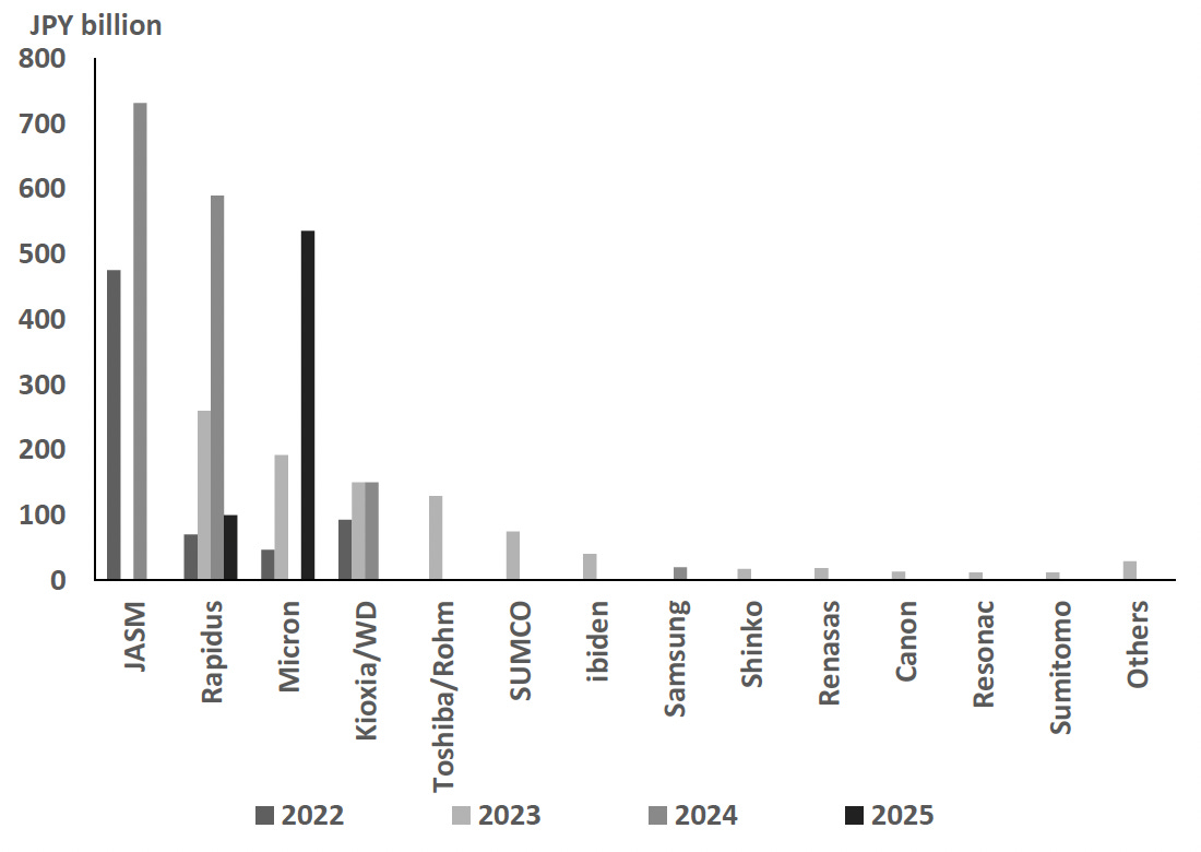
Exhibit 28: Japanese Government Subsidies to Semiconductor Firms (in JPY bn). Source: METI Japan, Business Deep Dives Research.
Indirect Competition, Geopolitics, and Long-Term Technological Risks
Beyond direct lithography rivals, ASML faces indirect competition from companies active in niche lithography, advanced packaging, and patterning-adjacent equipment, such as Veeco, EV Group, and SÜSS MicroTec. While these tools play important roles in specific manufacturing steps, particularly in specialty devices, compound semiconductors, and back-end processes, they do not represent functional substitutes for ASML’s core lithography systems. This distinction is reflected in the structure of the semiconductor ecosystem itself, where lithography equipment sits upstream of both fabrication and design. As illustrated by the broader industry ecosystem, advanced chip production, whether by foundries, integrated device manufacturers, or fabless players, ultimately depends on access to leading-edge fabrication tools, positioning ASML at a critical chokepoint regardless of where design or packaging innovation occurs.
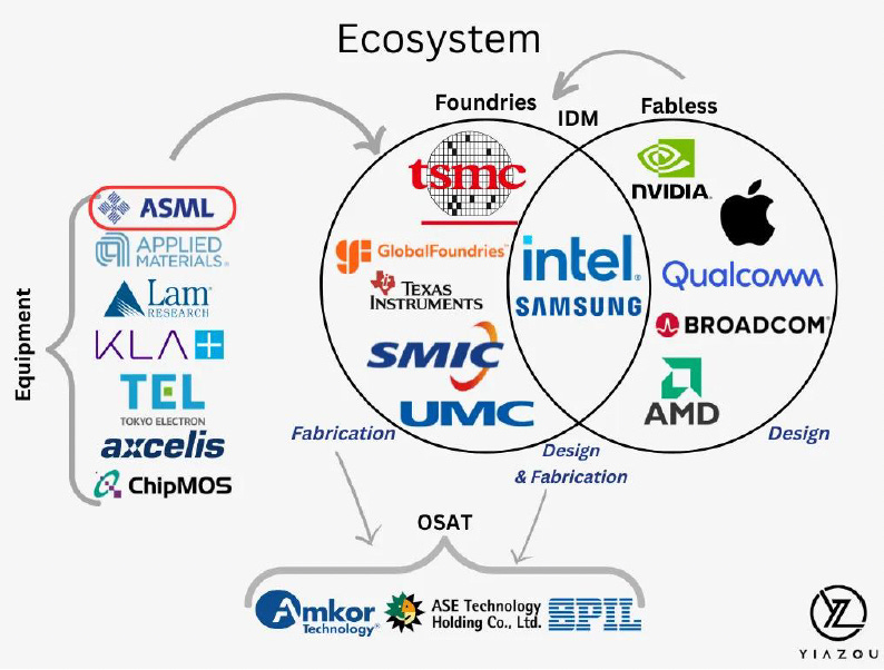
Exhibit 29: Semiconductor Ecosystem Overview Highlighting Lithography as the Structural Chokepoint in Advanced Chip Manufacturing. Source: Yiazou
Geopolitics represents the most significant source of uncertainty in ASML’s outlook, particularly through export controls that have effectively excluded China from EUV systems and increasingly restrict shipments of advanced DUV immersion tools. In the near term, these measures introduce revenue volatility and order-timing uncertainty. However, they do not materially alter ASML’s long-term strategic position. Leading-edge lithography demand remains concentrated among non-Chinese customers, most notably TSMC, Samsung, and Intel, whose technology roadmaps continue to depend on EUV and advanced DUV platforms. As a result, capacity and capital expenditure that might otherwise have been directed toward China have been absorbed elsewhere in the global semiconductor ecosystem. This is reflected in ASML’s evolving geographic revenue mix over time.
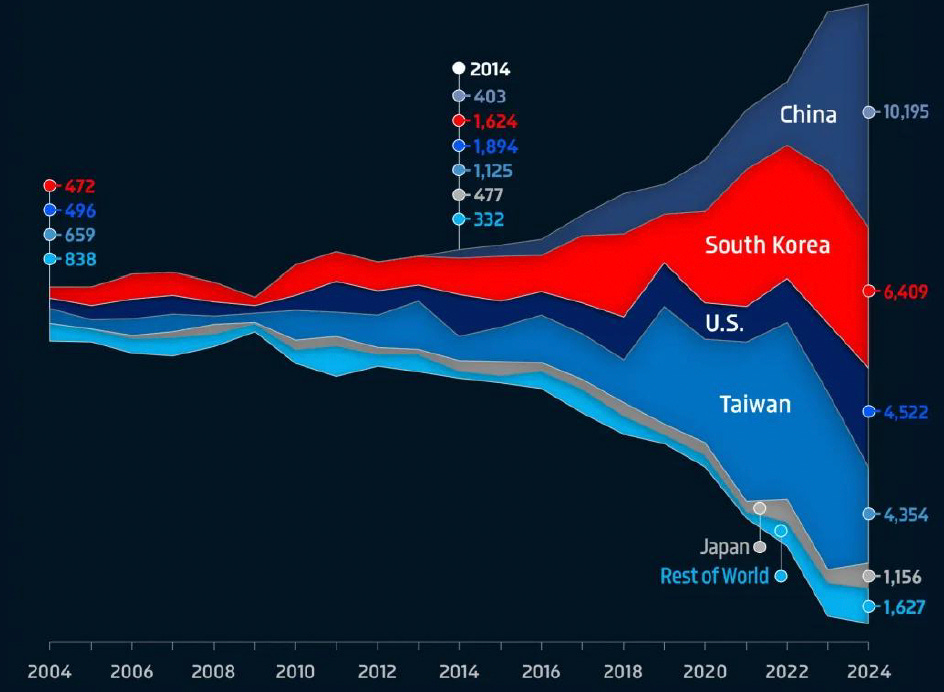
Exhibit 30: ASML Global Sales Revenue by Key Markets (2004-2024). Source: ASML Financial Statements, Econovis.
The exhibit illustrates the long-term evolution of ASML’s geographic revenue mix, highlighting the concentration of demand in leading-edge semiconductor manufacturing regions such as Taiwan, South Korea, and the United States, alongside rising but structurally different exposure to China. While China has emerged as ASML’s largest single geographic market in recent years, this demand is structurally concentrated in DUV systems and installed-base services rather than EUV-enabled leading-edge capacity. If this mix remains elevated over a prolonged period, ASML’s revenue profile could become more exposed to geopolitical intervention, export-control enforcement, and policy-driven ordering behavior, rather than technology-led node transitions. In contrast to Taiwan, South Korea, and the U.S., where demand is anchored in multi-node EUV roadmaps, China’s contribution carries higher regulatory and cyclicality risk, potentially increasing volatility in system sales and reducing the overall quality and visibility of ASML’s revenue mix over time.
ASML’s geographic mix is increasingly concentrated in leading-edge regions with EUV roadmaps, while elevated China exposure remains skewed toward DUV systems and services, carrying higher policy and cyclicality risk but without posing a credible near-term competitive threat at the leading edge
China’s domestic lithography capabilities remain multiple technology generations behind the leading edge, and the gap continues to widen as ASML advances into High-NA EUV. While incremental progress may occur in mature DUV technologies, the absence of a fully integrated ecosystem encompassing advanced optics, light sources, computational lithography, and process control significantly constrains China’s ability to challenge leading-edge lithography over the foreseeable horizon. However, China is urgently trying to develop its own lithography capabilities via SMEE (Shanghai Micro Electronics Equipment). As of late 2024, SMEE had progressed to a 90nm DUV scanner and was testing a 28nm immersion lithography tool. In fact, in early 2025 SMEE announced delivery of China’s first homegrown 28nm-capable scanner (the SSA800 series). While this is a notable achievement, these machines still lag behind ASML’s performance (in wafer throughput and critical dimension control) and are a decade or more behind in technology. There are also startups exploring alternative lithography approaches (e.g., multiprobe e-beam or particle-beam lithography), sometimes with high-profile backing, but none are near commercialization for high-volume manufacturing. This structurally positions China as a downstream participant rather than a near-term competitor at the frontier of semiconductor manufacturing.
Over the longer term, alternative exposure technologies such as nanoimprint, e-beam, or X-ray lithography represent theoretical substitution risks. However, these approaches remain peripheral due to fundamental limitations in throughput, defectivity, cost, and scalability that prevent adoption in high-volume manufacturing. Given the projected expansion of the lithography equipment market and the continued centrality of optical lithography to advanced fabrication flows, substitution risk is best viewed as long-dated to ASML’s core economic position.
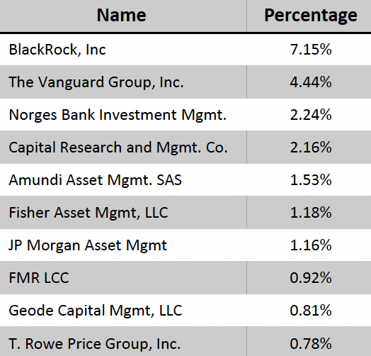
Exhibit 31: Top 10 Institutional Shareholders. Source: Business Deep Dives Research
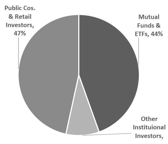
Exhibit 32: ASML Shareholding Pattern. Source: Business Deep Dives’ Research.
Management Overview
ASML’s executive leadership plays a pivotal role in steering the company’s strategy and sustaining its technological edge. The five-member Board of Management (led by the CEO as chair) is responsible for setting ASML’s objectives, executing its strategy, and overseeing day-to-day operations. The following are brief profiles of each member of ASML’s Board of Management:
Christophe Fouquet – President & Chief Executive Officer
Appointed CEO in 2024, he leads ASML’s overall strategic direction and operations. Fouquet has been a member of the Board of Management since 2018, previously heading ASML’s EUV lithography business and serving as Chief Business Officer. He joined ASML in 2008 after working at semiconductor equipment firms KLA-Tencor and Applied Materials. Fouquet holds a master’s degree in physics from the Institut Polytechnique de Grenoble.
Roger Dassen – Executive VP & Chief Financial Officer
As CFO, Dassen oversees ASML’s global finance, reporting and risk management. He joined ASML’s Board in 2018 after a nearly 28-year career at Deloitte, where he served as a Global Vice Chair and CEO of Deloitte Netherlands. Dassen brings extensive financial expertise and holds a PhD in business economics (along with master’s degrees in economics and auditing) from Maastricht University.
Frédéric Schneider-Maunoury – Executive VP & Chief Operations Officer
Schneider-Maunoury is responsible for ASML’s worldwide operations and manufacturing. He has served as COO since joining ASML in 2009 and became a Board member in 2010. He previously held senior leadership roles at Alstom (overseeing its hydro power and thermal products businesses) and earlier served in France’s Ministry of Trade and Industry. Schneider-Maunoury is a graduate of École Polytechnique (1985) and École Nationale Supérieure des Mines de Paris (1988).
Wayne Allan – Executive VP & Chief Strategic Sourcing & Procurement Officer
Allan leads ASML’s global supply chain and sourcing strategy, a role added to the Board of Management in 2023 to reflect the critical importance of supply chain performance. He joined ASML in 2018 after a 31-year career at Micron Technology, where he rose through various manufacturing and operations leadership positions to Senior VP of Global Manufacturing Operations. Allan holds a degree in chemical engineering from the College of Idaho.
Jim Koonmen – Executive VP & Chief Customer Officer
Koonmen heads ASML’s customer-facing functions, focusing on customer support and solutions. He joined ASML in 2007 via the acquisition of Brion Technologies and later served as CEO of Cymer (an ASML subsidiary) before leading ASML’s Applications business unit for five years. This background gives him deep experience in aligning ASML’s technology with customer needs. Koonmen holds dual M.S. degrees – one in Management from the MIT Sloan School of Management and another in Aeronautics & Astronautics from the Massachusetts Institute of Technology.
A Near-Monopoly Franchise with Durable Revenue Growth, Structural Margin Strength, and Robust Cash Conversion
ASML operates a near-monopoly franchise in the most critical step of advanced chip manufacturing, giving the company an unusually strong combination of pricing power, high switching costs, and deep customer lock-in. This strategic position supports a revenue model driven by leading-edge node migrations and wafer-fab capacity additions, which sustain demand for high-value lithography systems. In parallel, the steadily expanding installed base generates recurring service, spare parts, software, and upgrade revenue. Supported by these structurally strong segments, ASML has compounded its top-line at approximately 17% and 19% over the past ten and five years, respectively. Profitability remains structurally attractive, as the monopolistic nature of the business provides significant pricing power, enabling ASML to set prices according to the value delivered. Importantly, ASML’s healthy top-line growth, accompanied by strong and resilient margins, is further sustained by strong cash conversion, with the company consistently translating operating profit into meaningful free cash flow, supporting a shareholder returns framework that includes a recurring and growing dividend.
Steady Installed-Base Revenue, Innovation-Led Upside, and Cycle-Driven Volatility - Lithography remains a critical step in the wafer-fab process, and ASML’s near-monopoly position in the most advanced lithography nodes makes it a key enabler of leading-edge chip production. With few alternatives for advanced lithography, customer roadmaps are effectively constrained by ASML’s system availability and performance improvements, strengthening the company’s commercial leverage. However, ASML’s revenue remains materially linked to the broader wafer-fab equipment (WFE) and semiconductor capital expenditure (capex) cycle. Even when ASML is the only supplier for certain systems, foundries decide when to buy based on end-market demand, fab utilization, profitability, and the timing of new capacity buildouts. Given the high ASP and long lead times of lithography systems, customers retain meaningful flexibility to rephase delivery schedules or extend installation and qualification timelines to align with capex budgets and fab ramp plans.
A key quarterly indicator ASML reports is Net Bookings, which captures the value of new customer orders booked in the period and helps us gauge near-term demand and customer spending intent. In Q3 2025, ASML reported net bookings of €5.3 billion against systems revenue of €5.5 billion, implying a book-to-bill of 0.97x, suggesting order intake was broadly in line with shipments and that backlog was largely stable. The backlog stood at €33 billion as of Q3 2025, which equates to approximately six quarters of revenue coverage at the Q3 run-rate, providing strong forward visibility, even as quarterly results can still be influenced by system mix, customer delivery re-phasing, and the broader WFE spending cycle. The average book-to-bill ratio in the past eleven quarters is approximately 0.87x (with a range of 0.44x - 1.62x), and the order backlog has stepped down from €40.4 billion (as of Q4 2022), indicating a phase where ASML has been shipping against a historically strong order book while customers normalize incremental commitments. The post-COVID demand environment shifted from a sharp uplift in consumer electronics during 2021-2022 to an inventory correction, pricing pressure, and demand normalization across several semiconductor segments in 2023-2024. Furthermore, the past couple of years (2024-2025) have been increasingly shaped by the AI boom, which is sustaining spending on leading-edge logic and driving incremental investment in advanced DRAM capacity, but is also tempered by U.S.-China trade and tariff uncertainty that have caused chipmakers to stagger capex decisions, re-time system deliveries, and delay new orders despite strong long-term technology roadmaps. In practice chipmakers have become more selective with capex, prioritizing investments in leading-edge logic and advanced memory while emphasizing performance and productivity upgrades, node transition, and yield/throughput optimization over broad, volume-driven capacity expansion.
Exhibit 33: Net Bookings (in millions) and Book to Bill Ratio. Source: Company Data
ASML reported a revenue of €28.3 billion for the year ended 2024, compared to FY 2019 revenue of €11.8 billion, which corresponds to a 5-year CAGR of 19.0%. The year-on-year growth has broadly tracked underlying semiconductor industry dynamics, with significant immediate post-COVID total revenue growth (2020-2023 CAGR of 25%) driven by rising logic demand tied to digitalization trends such as 5G, cloud computing, and high-performance simulation and visualization workloads. This demand translated into accelerated technology roadmaps at major foundries and logic customers, supporting deeper adoption of advanced EUV systems and related productivity upgrades. By contrast, 2023-2025 has been characterized by a more normalized operating environment, with inventory digestion and more selective capital spending. Consistent with this shift, ASML posted -0.8% growth in net system sales and +2.6% growth in total sales in FY 2024, while the nine months ended 2025 shows a re-acceleration with +15.2% net system sales growth and +20.8% total sales growth, reflecting AI-led recovery in demand, improving shipment cadence and a mix skewing toward advanced EUV systems and performance-driven upgrades. With an estimated 80% share in the DUV lithography and a monopoly in the much more advanced EUV segment, ASML is already deeply penetrated across its core customer base.
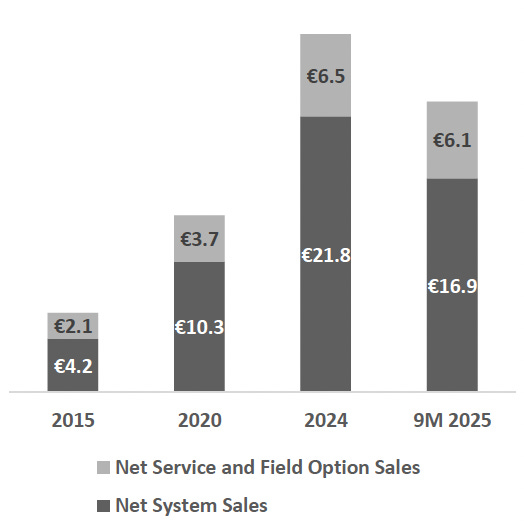
Exhibit 34: Historical Revenue Trend (in billion) Source: Company Data
In the near term, growth is likely to be shaped more by capex timing and geographic mix, as tariff and trade-policy uncertainty can cause customers to delay commitments, with uncertainty surrounding the company’s future revenue contributions from China. Revenue from China has scaled significantly in the past three years, from contributing 13.8% of total revenue in 2022 to 36.1% in 2024. For 2025, China contributed 27% of total system sales for Q1 and Q2, and 42% in Q3 2025. During a time when the global demand for advanced lithography systems was going through a normalization phase with major chip manufacturers adjusting their capital spending, China’s DUV demand effectively became a counter-cyclical offset. However, the durability of these contributions remains uncertain, as it is highly likely to be heavily influenced by policy and timing effects rather than broad-based end-market expansion. Management has explicitly indicated that China’s revenue contribution is expected to decline meaningfully from the elevated levels seen in 2023 and 2024, supporting the view that recent strength is unlikely to be sustained at the same scale over the medium term.
Over the long term, ASML’s growth should be driven primarily by technology intensity and broader wafer-fab equipment (WFE) and semiconductor capex cycle. Management has reiterated a 2030 revenue opportunity of approximately €44 billion to €60 billion, implying a revenue CAGR of 7.6% to 13.4% from the €28.3 billion base in FY 2024. This long-range path is supported by increasing lithography spending at future nodes, continued EUV mix shift and productivity upgrades, the ramp of High-NA, and sustained AI-driven investment in leading-edge logic and advanced memory, with installed-base services providing an additional layer of recurring growth and visibility.

Exhibit 35: Net System Sales - No. of Units. Source: Company Data
Structural Moat Supports Margin Resilience With Incremental Expansion From Mix and Cost Leverage: ASML’s margin profile is anchored in its structural moat, with lithography’s mission-critical role and limited competitive alternatives supporting durable pricing discipline. As a result, gross margins have remained structurally resilient. Gross margins held broadly in the 44.7% to 46.1% range during 2015-2019, a period marked by solid growth in the DUV and service/field option revenue alongside the early ramp of EUV systems. In 2020, EUV economics improved significantly as volumes scaled and the platform progressed through the learning curve, enabling ASML to capture a more favorable mix and achieve better cost absorption. This shift helped drive approximately 3.5% gross margin expansion to 48.9%. Building on the step-up in 2020, ASML’s gross margin expanded further to 52.7% in 2021, reflecting not just higher EUV volumes but a clear improvement in mix and profitability. Management attributed the expansion to improved EUV profitability, a richer DUV product mix, and higher installed-base profitability. Following this inflection, gross margin has broadly stabilized in the 50.5%-51.3% range during 2022-2024, suggesting that the initial EUV profitability uplift and installed-base improvement have largely normalized into the run-rate. In the nine months ended 2025, the gross margin improved to 52.7%, reflecting a more favorable mix and stronger upgrade activity. Management continues to guide toward a structurally higher margin profile over time, targeting a 56%-60% margin by 2030 as EUV and High-NA scale and installed-base monetization deepen.
As ASML has scaled, operating leverage has amplified the improvement in gross margins and translated it into even faster growth in operating profitability. Operating margin expanded from 23.6% in 2015 to 29.0% in 2020, and further to 31.9% in 2024, reflecting a stronger gross profit flow-through and disciplined growth in operating expenses. The nine months ended 2025 financial results show a further expansion to 34.9%. Over the past nine years, gross profit compounded at 19.6%, while operating profit grew at a higher 22.2% CAGR, reflecting disciplined opex growth relative to revenue. While operating-margin expansion has broadly tracked the gross-margin trajectory, the magnitude of operating leverage has resulted in a meaningfully faster growth rate in EBIT. Looking ahead, with management targeting 56%-60% gross margin by 2030 on the back of a richer product mix, we anticipate meaningful scope for incremental operating leverage, which could support EBIT margin expansion to potentially near the 40% level in the longer term.
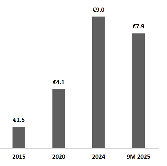
Exhibit 36: Operating Income (in billions). Source: Company Data
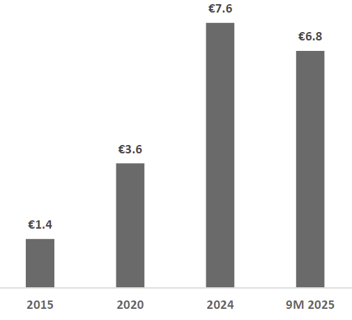
Exhibit 37: Net income (in billion). Source: Company Data.
Consistent Capital Returns Supported by Robust Net Cash and Strong Free-Cash-Flow Conversion: ASML’s strong historical growth and structurally attractive, resilient margin profile are complemented by high cash conversion, with the company consistently translating reported earnings into operating cash flow and then into meaningful free cash flow after funding capex and sustained R&D investment. Over the past nine years, ASML has converted all of its accounting earnings into operating cash, with the CFO exceeding net income in seven of the past nine years, emphasizing the strength of its cash earnings. The median and average CFO to net income ratios of 1.27x and 1.26x, respectively, indicate consistently strong cash realization, supported by healthy profitability and disciplined working capital management. Importantly, cash generation has scaled in tandem with earnings, with both CFO and net income compounding at a 21% CAGR over the period. Even with a steady reinvestment program, capex has remained around 6% of revenue (or 19% of operating cash flow) and has also grown at roughly 21% CAGR, allowing free cash flow to compound at a similar 21% CAGR. This combination of strong conversion, measured reinvestment, and scalable cash generation supports ASML’s ability to maintain consistent shareholder returns through dividends and buybacks while continuing to invest through the cycle.
Over the past nine years, ASML has returned approximately €30 billion to shareholders through a combination of dividends and share repurchases. The dividend has increased at an estimated 26% CAGR, while buybacks have been executed through multi-year programs, providing a flexible mechanism to return excess cash while maintaining the capacity to invest in EUV and High-NA. At the end of Q3 2025, the company reported €5.1 billion in cash and cash equivalents against a total debt of €2.7 billion. This results in a net cash position of €2.4 billion (7.5% of TTM revenue). This balance-sheet strength supports the company’s ability to fund strategic capex and R&D, while continuing to return capital to shareholders via a stable dividend and opportunistic buybacks.
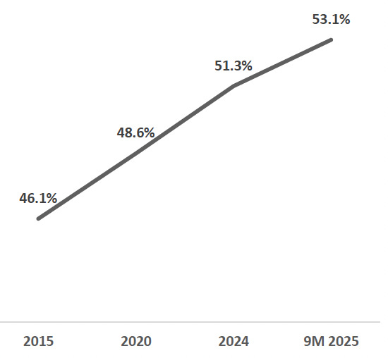
Exhibit 38: Gross Margins. Source: Company Data
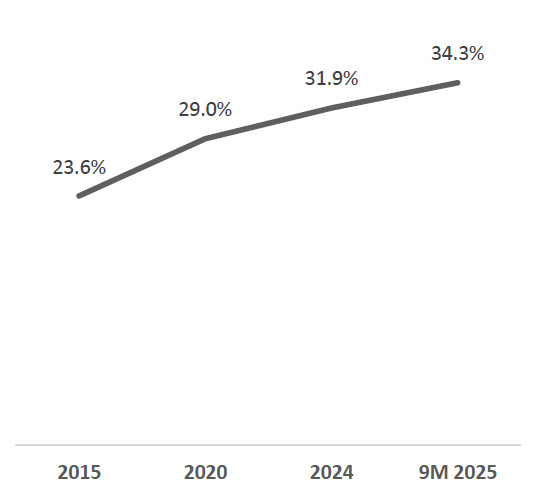
Exhibit 39: Operating Margins. Source: Company Data
Revenue Build, Margin Trajectory, and Key Modeling Assumptions
ASML’s near-monopoly in lithography effectively ties its growth to the industry’s overall spending on lithography equipment and the ongoing evolution of its product mix toward higher-value platforms. As leading-edge nodes become more complex, a larger share of industry capex shifts toward advanced systems, particularly EUV and related productivity upgrades, which increases both the revenue opportunity per fab and ASML’s value capture per node transition. With a top-down approach towards revenue forecasting, we begin by estimating global wafer fab equipment (WFE) spending and then allocate a portion of that total to lithography, applying an industry-based estimate of approximately 30% of WFE spend. We then translate this lithography spend into ASML revenue by applying EUV and DUV market-share assumptions, separating the pool into system sales and installed-base-related revenue, and layering in unit economics and pricing inputs such as tool ASPs and shipment volumes to build a structured revenue bridge. Using this framework, we estimate the total lithography spending of approximately €28.55 billion in 2025. Incorporating our assumption on market growth, EUV and DUV unit shipments, and average selling prices for each segment, we derive the combined EUV and DUV system sales of approximately €23.14 billion for 2025 and a total revenue estimate of €32.24 billion. Given the uncertainty around tariffs and the sustainability of China-driven demand, combined with management’s guidance that China’s revenue contribution should normalize at a lower level from the elevated 2024-2025 levels, we have taken a more cautious stance in our forward build. Accordingly, we apply conservative growth and mix assumptions and arrive at a 2026 estimate of €33.43 billion. Post 2024, we expect growth to be driven primarily by structural technology trends rather than geographic or policy-related factors. AI-led investment should continue to support demand for leading-edge logic, while rising lithography intensity at advanced nodes drives a sustained mix toward EUV, High-NA, and productivity upgrades. In line with these drivers and management’s 2030 revenue target of €44 - €60 billion, we estimate 2030 revenue of approximately €55 billion, reflecting sustained structural growth.
ASML has maintained a consistently strong and resilient margin profile over the past decade. With 2025 expected to close on a robust note, we estimate a 52.6% gross margin and a 33.8% operating margin. In 2026, we anticipate some normalization as the elevated, high-margin immersion shipments to China moderate, which we model as a contraction of approximately 140 bps in both gross and operating margins. Beyond these near-term headwinds, we expect profitability to re-accelerate as the revenue mix shifts further toward EUV, productivity upgrades, and higher-margin installed-base services, while operating leverage improves as incremental gross profit flows through a largely scalable cost structure. On this basis, we forecast a gross margin of approximately 56% and an operating margin of 40% by 2030, consistent with management’s long-term margin targets and a richer mix of advanced lithography and recurring service revenue.
In our forecast, we adopt a conservative capital allocation stance that prioritizes reinvestment over shareholder distribution. We do not explicitly model dividends or share buybacks; instead, we assume that internally generated cash flows are retained on the balance sheet or redeployed to support long-term growth initiatives. While trailing two-year quarterly capex has averaged approximately 6.5% of revenue, we assumed a normalized 5.0% of revenue in our forward estimates, reflecting improved capital efficiency as recent capacity expansions mature and incremental investment requirements moderate.
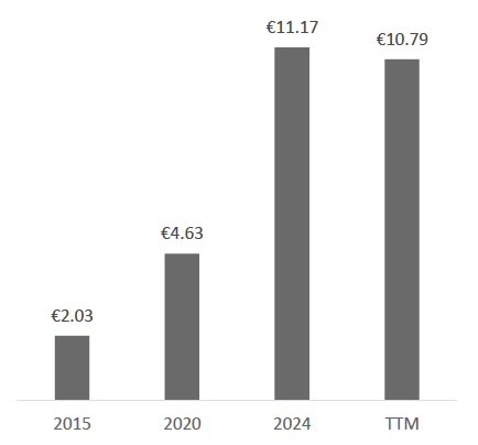
Exhibit 40: Cash Flow From Operations (in € billion). Source: Company Data
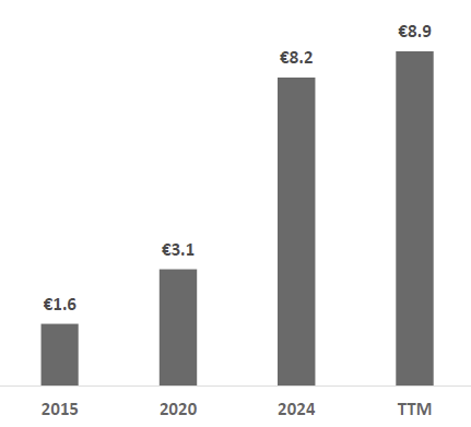
Exhibit 41: Free Cash Flow (in € billion). Source: Company Data
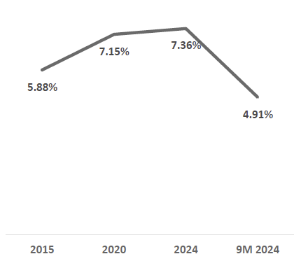
Exhibit 42: Capex As A % Of Revenue. Source: Company Data.
The complete financial statements, forward projections, valuation model, and scenario analyses are included in the PDF version of this report as well as the financial model. Click here to view (pages 30-36, Exhibits 43-56).
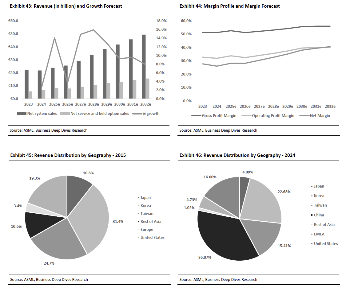
Final Words, and Valuation
Lithography is the step that “writes” the chip, printing the microscopic circuit patterns onto silicon and setting the hard ceiling for how small, fast, power-efficient, and high-yield a semiconductor can be. As nodes shrink, lithography becomes the limiting bottleneck because dozens of layers must be patterned and aligned with extreme precision, and any loss in accuracy or throughput directly hits yield, cost, and time-to-ramp. ASML therefore matters more than a typical equipment supplier because it dominates the enabling tools for both cutting edge and the volume base of global production, holding 100% market share in EUV, the only commercially proven lithography technology capable of manufacturing the most advanced logic used in AI accelerators, high-performance computing (HPC), and next-generation communications, and approximately 80% share in DUV, which remains essential for most mature node chips and for many critical layers even in advanced processes. When you combine this technological dominance with long qualification cycles and extremely high switching costs, ASML ends up as a true choke point for global semiconductor progress and capacity expansion, which is why governments, foundries, and the entire supply chain treat it as a company with outsized national and global importance. ASML’s technological leadership is the foundation of its moat and positions the company as a high-quality, mission-critical franchise within the semiconductor value chain. These attributes clearly make ASML an exceptional business, but the relevant investor question is whether it is an attractive opportunity at the current valuation. Answering that requires assessing how much of ASML’s long-term earnings power is already reflected in the current price. This depends on the durability of AI-led leading-edge demand, the mix-shift toward higher-value EUV and High-NA systems, the growing installed-base services stream, and management’s guided margin and growth trajectory. At the same time, investors must account for near-term volatility arising from semiconductor capex phasing and near-term policy-driven uncertainty around the regional mix.
We estimate ASML’s intrinsic value using a Discounted Cash Flow framework, forecasting free cash flows based on the operating assumptions outlined previously while applying a discount rate of 8.05% and a terminal growth rate of 1.5%. Given ASML’s near-monopoly positioning in lithography, strong structural moat, and ability to manage near-term industry cyclicality and policy-related headwinds, we view our assumptions as conservatively constructed, anchored to management’s long-term guidance and reasonable industry growth expectations. Based on these assumptions, our DCF implies an intrinsic equity value of $1,239 per share, implying an upside of 15.8%.
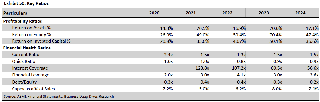
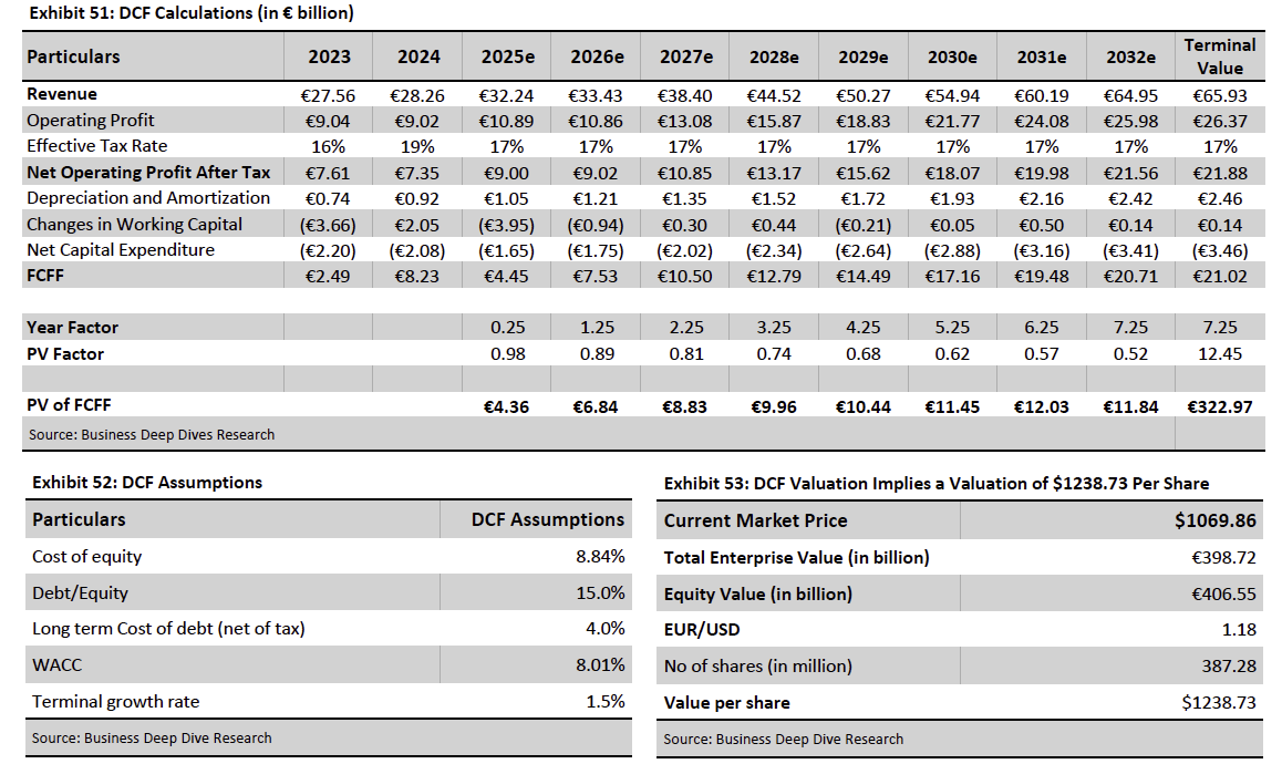
Risks and Concerns
Dependence on Limited Product Sales and Cyclical Semiconductor Demand: ASML derives most of its revenue from the sale of a relatively small number of lithography systems (e.g., 418 units in 2024) to a small number of customers, making results highly sensitive to shipment timing and customer investment cycles. Shipment delays, changes in order timing, or revenue recognition impacts (including fast-shipments requiring on-site acceptance) can materially affect period-to-period comparability. Slowdowns in global semiconductor capex (driven by macroeconomic uncertainty, interest rates, or industry overcapacity) could significantly reduce demand.
Increasing Competitive Intensity and Technological Substitution Risks: ASML faces strong competition in DUV lithography from Canon and Nikon, both with deep patent portfolios and financial scale. Furthermore, geopolitical motives for technology self-sufficiency are encouraging new regional competitors, while alternative semiconductor manufacturing approaches may reduce the reliance on lithography-based scaling. As competitive alternatives emerge, pricing pressure and potential market share erosion could impact growth.
Uncertainty Around R&D Execution and Next-Generation Technology Development: The success of ASML’s growth strategy hinges on the timely and cost-effective execution of advanced R&D programs, including EUV, High-NA EUV, and multibeam technologies. Delays in ASML’s or suppliers’ development roadmaps, or customer reluctance to adopt new architectures, can hinder product launches and reduce returns on significant R&D investments. If new technologies fail to meet performance expectations or are adopted slower than anticipated, profitability and competitive positioning may suffer.
Intellectual Property Theft, Leakage, or Infringement Exposure: ASML relies heavily on protecting its proprietary know-how, yet the company faces increasing cyber threats and risks of misappropriation across its innovation ecosystem. Breaches of confidentiality agreements, expiration of key patents, or inadequate legal protection in certain jurisdictions could reduce ASML’s technology lead. Legal disputes over IP rights can be costly, resource-intensive, and disruptive to operations.
Cybersecurity Vulnerabilities and IT System Disruptions: ASML recognizes that cyberattacks, malware, or unintended software exposures could severely impact operations or even transmit disruptions to customer environments. As the company’s global footprint and visibility increase, the threat profile intensifies, with risks ranging from data breaches to operational shutdowns. Large-scale IT projects (e.g., ERP migration) or AI-related system changes may introduce additional risks of failure or unintended outcomes.
Regulatory, Export Control, and Compliance Exposure Across Jurisdictions: ASML operates under a complex international regulatory environment involving export controls, national security rules, ESG requirements, product compliance, tax regulations, and antitrust laws. As operations expand globally, ensuring full compliance becomes more challenging, increasing the likelihood of inadvertent violations despite rigorous internal controls. Changes in export restrictions, especially for advanced lithography tools, may limit access to key markets or delay shipments.
Macroeconomic, Geopolitical, and Financial Market Volatility: Global inflation, rising interest rates, geopolitical tensions, and capital market volatility influence both customer investment cycles and ASML’s internal cost structure. Customers may delay or reduce equipment purchases in uncertain environments, while financing conditions may deteriorate for both ASML and its clients. Major geopolitical events, including export controls, trade disputes, or conflicts, may disrupt supply chains, introduce regulatory burdens, or negatively affect long-term demand.
We appreciate your time in reading our Dexcom Deep Dive. We will continue tracking its performance and strategic evolution through periodic updates and implication reports available to subscribers.
Disclosures and Disclaimers
This report is for informational and educational purposes only and does not constitute investment advice, a recommendation, or a solicitation to buy or sell any securities. All opinions expressed reflect the author’s judgment as of the publication date and are subject to change without notice.
The author does not currently hold shares of ASML Holdings (ASML) but may initiate a position in the future without further notice.
For the full disclaimer, click here.
Copyright © 2025 Business Deep Dives. All rights reserved.
Business Deep Dives is an independent research publication operating on a pre-incorporation basis. All content is protected under applicable international copyright principles.